CY29973AIT

CY29973
Document #: 38-07291 Rev. *C Page 4 of 9
Description
The CY29973 has an integrated PLL that provides low-skew and
low-jitter clock outputs for high-performance microprocessors.
Three independent banks of four outputs and an independent
PLL feedback output, FB_OUT, provide exceptional flexibility for
possible output configurations. The PLL is ensured stable
operation given that the VCO is configured to run between 200
MHz to 480 MHz. This allows a wide range of output frequencies
up to125 MHz.
The phase detector compares the input reference clock to the
external feedback input. For normal operation, the external
feedback input, FB_IN, is connected to the feedback output,
FB_OUT. The internal VCO is running at multiples of the input
reference clock set by FB_SEL(0:2) and VCO_SEL select inputs,
refer to Table 1 on page 1. The VCO frequency is then divided
down to provide the required output frequencies. These dividers
are set by SELA(0,1), SELB(0,1), SELC(0,1) select inputs, see
Table 2. For situations were the VCO needs to run at relatively
low frequencies and hence might not be stable, assert VCO_SEL
LOW to divide the VCO frequency by 2. This maintains the
desired output relationships, but provides an enhanced PLL lock
range.
The CY29973 is also capable of providing inverted output clocks.
When INV_CLK is asserted high, QC2 and QC3 output clocks
are inverted. These clocks could be used as feedback outputs to
the CY29973 or a second PLL device to generate early or late
clocks for a specific design. This inversion does not affect the
output to output skew.
Zero Delay Buffer
When used as a zero delay buffer the CY29973 is likely to be in
a nested clock tree application. For these applications the
CY29973 offers a low voltage PECL clock input as a PLL
reference. This allows the user to use LVPECL as the primary
clock distribution device to take advantage of its far superior
skew performance. The CY29973 then can lock onto the
LVPECL reference and translate with near zero delay to low
skew outputs.
By using one of the outputs as a feedback to the PLL the propa-
gation delay through the device is eliminated. The PLL works to
align the output edge with the input reference edge thus
producing a near zero delay. The reference frequency affects the
static phase offset of the PLL and thus the relative delay between
the inputs and outputs. Because the static phase offset is a
function of the reference clock the Tpd of the CY29973 is a
function of the configuration used.
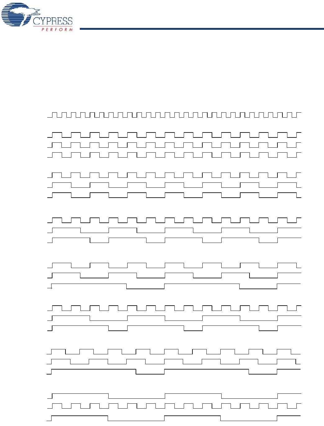
Glitch-Free Output Frequency Transitions
Customarily when output buffers have their internal counter’s
changed “on the fly’ their output clock periods will:
1. Contain short or “runt” clock periods. These are clock cycles
in which the cycle(s) are shorter in period than either the old
or new frequency that is being transitioned to.
2. Contain stretched clock periods. These are clock cycles in
which the cycle(s) are longer in period than either the old or
new frequency that is being transitioned to.
This device specifically includes logic to guarantee that runt and
stretched clock pulses do not occur if the device logic levels of
any or all of the following pins changed “on the fly” while it is
operating: SELA, SELB, SELC, and VCO_SEL.
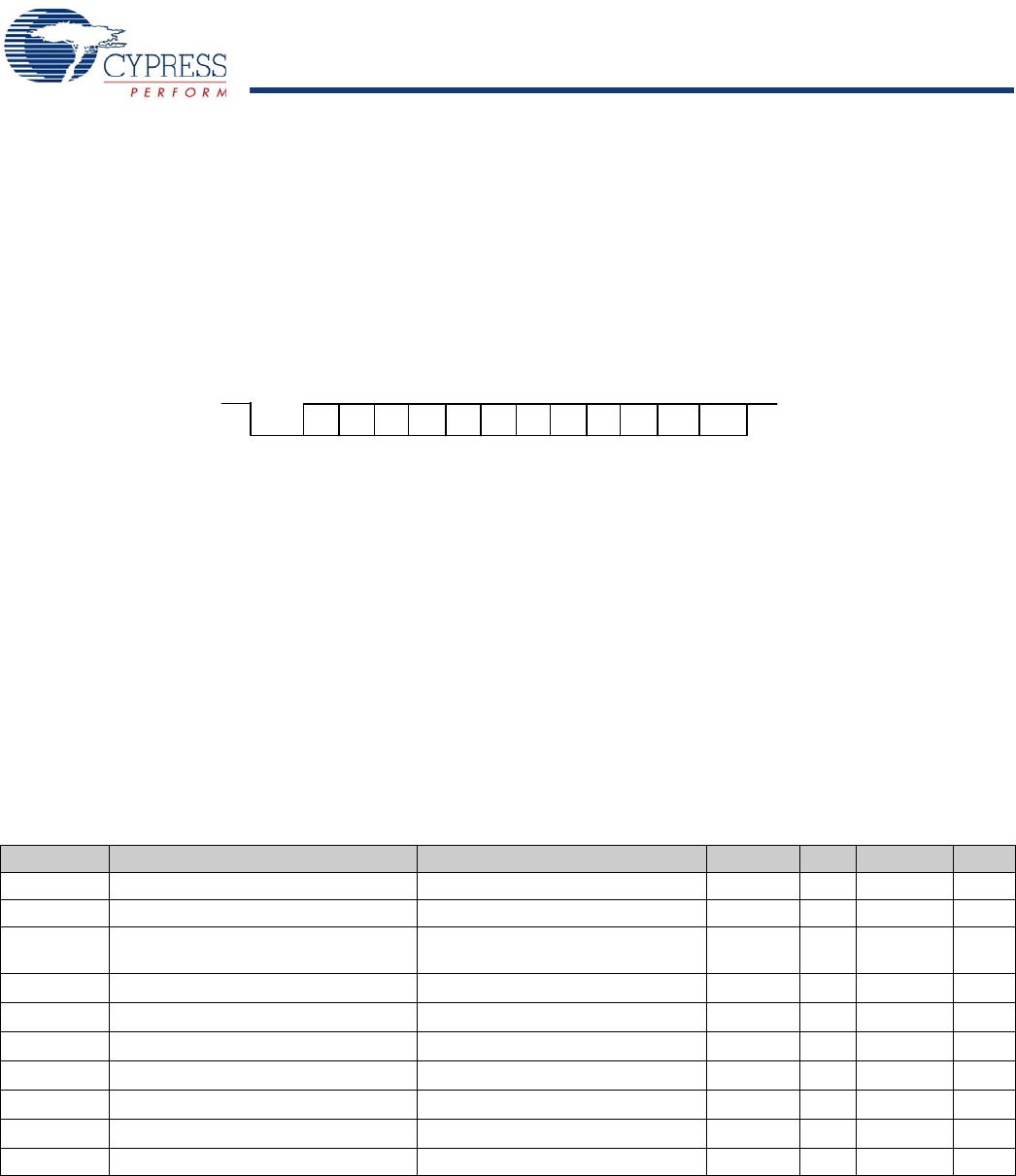
Table 2. Divider Table
VCO_SEL SELA1 SELA0 QA SELB1 SELB0 QB SELC1 SELC0 QC
0 0 0 VCO/8 0 0 VCO/8 0 0 VCO/4
0 0 1VCO/120 1VCO/120 1 VCO/8
0 1 0VCO/161 0VCO/161 0VCO/12
0 1 1VCO/241 1VCO/201 1VCO/16
1 0 0 VCO/4 0 0 VCO/4 0 0 VCO/2
1 0 1 VCO/6 0 1 VCO/6 0 1 VCO/4
1 1 0 VCO/8 1 0 VCO/8 1 0 VCO/6
1 1 1VCO/121 1VCO/101 1 VCO/8
[+] Feedback
CY29973
Document #: 38-07291 Rev. *C Page 5 of 9
SYNC Output
In situations were output frequency relationships are not integer multiples of each other the SYNC output provides a signal for system
synchronization. The CY29973 monitors the relationship between the QA and the QC output clocks. It provides a low going pulse,
one period in duration, one period prior to the coincident rising edges of the QA and QC outputs. The duration and the placement of
the pulse depend on the higher of the QA and QC output frequencies. The following timing diagram illustrates various waveforms for
the SYNC output. Note that the SYNC output is defined for all possible combinations of the QA and QC outputs even though under
some relationships the lower frequency clock could be used as a synchronizing signal.
Figure 1. SYNC Output for Different Input and Out Ratio
[+] Feedback
CY29973
Document #: 38-07291 Rev. *C Page 6 of 9
Power Management
The individual output enable or freeze control of the CY29973 allows the user to implement unique power management schemes into
the design. The outputs are stopped in the logic ‘0’ state when the freeze control bits are activated. The serial input register contains
one programmable freeze enable bit for 12 of the 14 output clocks. The QC0 and FB_OUT outputs can not be frozen with the serial
port, this avoids any potential lock up situation must an error occur in the loading of the serial data. An output is frozen when a logic
‘0’ is programmed and enabled when a logic ‘1’ is written. The enabling and freezing of individual outputs is done in such a manner
as to eliminate the possibility of partial “runt” clocks.
The serial input register is programmed through the SDATA input by writing a logic ‘0’ start bit followed by 12 NRZ freeze enable bits.
The period of each SDATA bit equals the period of the free running SCLK signal. The SDATA is sampled on the rising edge of SCLK.
Figure 2. Control Bit Map
Absolute Maximum Conditions
[3]
Maximum Input Voltage Relative to V
SS
:.............. V
SS
- 0.3V
Maximum Input Voltage Relative to V
DD
:............. V
DD
+ 0.3V
Storage Temperature:................................- 65°C to + 150°C
Operating Temperature:................................- 40°C to +85°C
Maximum ESD protection............................................... 2 kV
Maximum Power Supply:................................................5.5V
Maximum Input Current:................................................ ± 20 mA
This device contains circuitry to protect the inputs against
damage due to high static voltages or electric field; however,
precautions must be taken to avoid application of any voltage
higher than the maximum rated voltages to this circuit. For proper
operation, V
in
and V
out
must be constrained to the range:
V
SS
< (V
in
or V
out
) < V
DD
Unused inputs must always be tied to an appropriate logic
voltage level (either V
SS
or V
DD
).
D0 D1 D2 D3 D4 D5 D6 D7 D8 D9 D10 D11
D0-D3 are the control bits for QA0-QA3, respectively
D4-D7 are the control bits for QB0-QB3, respectively
D8-D10 are the control bits for QC1-QC3, respectively
D11 is the control bit for SYNC
Start
Bit
DC Electrical Specifications V
DD
= 2.9V to 3.6V, V
DDC
= 3.3V ±10%, T
A
= - 40°C to +85°C
Parameter Description Conditions Min Typ. Max Unit
V
IL
Input Low Voltage V
SS
–0.8V
V
IH
Input High Voltage 2.0 V
DD
V
V
PP
Peak-to-Peak Input Voltage
PECL_CLK
300 1000
mV
V
CMR
Common Mode Range PECL_CLK
[4]
V
DD
– 2.0 V
DD
– 0.6
V
I
IL
Input Low Current
[5]
–120
μA
I
IH
Input High Current
[5]
––120
μA
V
OL
Output Low Voltage
[6]
I
OL
= 20 mA 0.5 V
V
OH
Output High Voltage
[6]
I
OH
= –20 mA 2.4 V
I
DDQ
Quiescent Supply Current
–1015mA
I
DDA
PLL Supply Current V
DD
only 15 20 mA
Notes
3. Multiple Supplies: The voltage on any input or IO pin cannot exceed the power pin during power up. Power supply sequencing is NOT required.
4. The V
CMR
is the difference from the most positive side of the differential input signal. Normal operation is obtained when the “High” input is within the V
CMR
range
and the input lies within the V
PP
specification.
5. Inputs have pull up/pull down resistors that effect input current.
6. Driving series or parallel terminated 50Ω (or 50Ω to V
DD
/2) transmission lines.
[+] Feedback

CY29973AIT

Mfr. #:
Manufacturer:
Cypress Semiconductor
Description:
Phase Locked Loops - PLL 3.3V,125MHz,LVPECL/ LVCMOS In,12 Out
Lifecycle:
New from this manufacturer.
Delivery:
DHL FedEx Ups TNT EMS
Payment:
T/T Paypal Visa MoneyGram Western Union

Products related to this Datasheet