LT3003
4
3003fa
PIN FUNCTIONS
TYPICAL PERFORMANCE CHARACTERISTICS
LED1 (Pin 1): Controlled current input for a string of LEDs
with a cathode lead connected to the pin. Connect the fi rst
string of LEDs to this pin.
LED2 (Pin 2): Controlled current input for a string of LEDs
with a cathode lead connected to the pin. Connect the sec-
ond string of LEDs to this pin.
LED3 (Pin 3): Controlled current input for a string of LEDs
with a cathode lead connected to the pin. Connect the third
string of LEDs to this pin.
V
MAX
(Pin 4):
• Boost: Connect to V
OUT
• Buck Mode: Connect to Input Supply
• Buck-Boost Mode: Connect to V
OUT
V
IN
(Pin 5): Input Supply, Upper Rail. This pin must be
locally bypassed with a capacitor to ground. V
IN
powers
the internal control circuitry.
• Boost: Connect to Input Supply
• Buck Mode: Connect to Input Supply
• Buck-Boost Mode: Connect to V
OUT
PWM (Pin 6): Input Pin for PWM Dimming Control. A
PWM signal above 0.5V (on threshold) turns the LT3003
channels on. A PWM signal below 0.5V completely discon-
nects each LED string. If the application does not require
PWM dimming, then the PWM pin can be left either open
(an internal 10µA source current pulls PWM high) or it
can be connected to a supply between 0.5V to 15V.
OT1 (Pin 7): Overtemperature Output. OT1 pulls 100µA
from the pin when the junction temperature exceeds
125°C. The part has to cool down by 6°C for the fl ag to
reset; ideal for providing an overtemperature fl ag to the
system microprocessor.
OT2 (Pin 8): Overtemperature Output. OT2 Pulls 300µA
from the pin when the junction temperature exceeds
125°C. The part has to cool down by 6°C for the fl ag to
reset; ideal for connecting to the switching regulator g
m
error amplifi er output to defeat switching.
SHDN (Pin 9): Micropower Shutdown Pin. Below 0.7V
shuts down the IC. Typically I
VIN
= 4µA for SHDN = 0V.
Boost: Connect to System Shutdown Signal or V
IN
Buck Mode: Connect to System Shutdown Signal
or V
IN
Buck-Boost Mode: If PWM dimming, connect to PWM
(Pin 6); if no PWM dimming, connect to system shut-
down signal or V
IN
V
IN
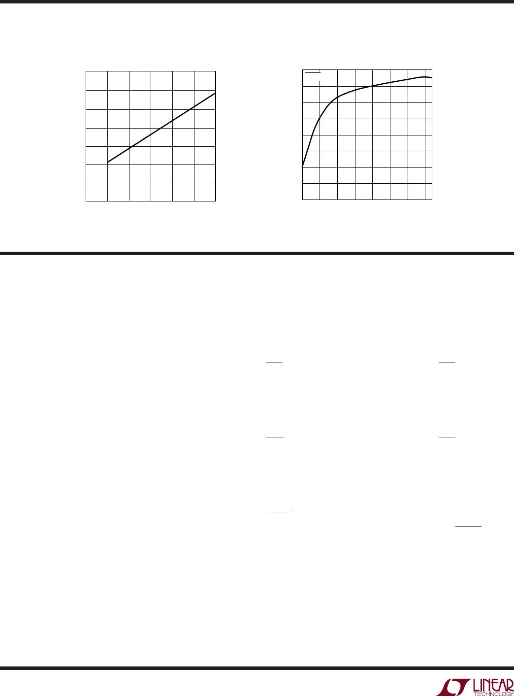
Quiescent Current vs I
LED
V
IN
Shutdown Current vs V
IN
I
LED
(mA)
50
35
30
25
20
15
10
5
0
200 300
3003 G07
100 150
250 350
V
IN
QUIESCENT CURRENT (mA)
V
IN
(V)
3
V
IN
SHUTDOWN CURRENT (µA)
8
12
3003 G08
4
0
13
23
33
8
18
28
38
16
6
10
2
14
SHDN = 0
T
A
= 25°C unless otherwise noted.
LT3003
5
3003fa
BLOCK DIAGRAM
Figure 1. Block Diagram
1 2
+
+
+
4
V
EE
B1 B2 B3
LED1
PWM
0.5V
V
MAX
LED2
11
EXPOSED PAD
LED3
3
V
IN
3V
5
V
EE
SHDN
0.7V
9
OT1
7
PWM
LOGIC
THERMAL
SHUTDOWN
BIAS
BGBG 125°C
150°C
OT2
3003 F01
8
6
+
10
+
B2B1
V
IN
B3
V
EE
(Pin 10): Lower Rail.
• Boost: Connect to System Ground
• Buck Mode: Connect to Inductor
• Buck-Boost Mode: Connect to Input Supply
Exposed Pad (Pin 11): GND. The ground for the IC should
be soldered to a continuous copper ground plane under
the LT3003 die. Soldering the Exposed Pad to the copper
ground plane under the device will reduce thermal resis-
tance and increase the power capability of the LT3003.
PIN FUNCTIONS
LT3003
6
3003fa
The LT3003 is an easy-to-use 3-channel LED ballaster.
It allows three strings of LEDs to be driven in parallel
with accurate LED current matching. A PWM pin is also
provided allowing LED currents to be turned on and off at
very low duty cycles for very wide LED dimming ranges.
For reliable system thermal management, two output fl ags,
OT1 and OT2, are provided to indicate when the junction
temperature exceeds 125°C.
The Block Diagram in Figure 1 best illustrates the features
of LT3003. The LT3003 internal bias circuitry is turned on
when V
IN
> 3V and SHDN > 0.7V. For LED current to be
active in each channel, the PWM pin must exceed 0.5V.
V
MAX
should be connected to the highest supply in the
application (see various application modes of boost, buck,
buck-boost in the Typical Applications section).
The LT3003 ballasting feature is achieved by using the
current monitored in the LED2 channel to control the
current in channels LED1 and LED3. A servo loop exists
for each channel LED1 and LED3 that compares the cur-
rent in each channel to the LED2 reference channel. The
current in LED2 channel is determined by the LED current
programmed by the partner LED driver. Details of how LED
current can be programmed by the partner IC are covered
in the Typical Applications section using various ICs as
LED drivers. Maximum fault current in each of the LT3003
LED pins is internally limited to 550mA. If any LED string
experiences an open-circuit fault, all LED string currents
are turned off.
The LT3003 PWM pin has unique level-shifting circuitry to
allow a simple logic-level PWM signal to turn each LED pin
current on and off regardless of the V
EE
pin voltage. This
allows very simple PWM dimming control of LED current
without any need for external level-shifting components
in buck mode and buck-boost mode applications. Care is
taken to ensure low current (nano amps) in the V
EE
and
V
MAX
pins 10µs after PWM low edge. This feature mini-
mizes leakage currents in each application to maximize
PWM dimming ratio. Details of PWM dimming and criti-
cal parameters are given in the Applications Information
section PWM Dimming.
The LT3003 incorporates internal junction temperature
sensing and provides two open-collector outputs, OT1
and OT2, which become active low when junction tem-
perature exceeds 125°C. OT1 is sized to pull 100µA and
can be used as an input to the microprocessor for system
thermal management. OT2 is sized to pull 300µA to defeat
switching for most of LTC’s LED drivers by pulling down
the g
m
error amplifi er output. LT3003 is forced to a “zero
LED current state” by a special internal protection circuit
when junction temperature reaches 150°C.
To calculate the LT3003 junction temperature, see Thermal
Calculations in the Applications Information section.
OPERATION
LT3003EMSE#TRPBF

Mfr. #:
Manufacturer:
Analog Devices / Linear Technology
Description:
LED Lighting Drivers Three Channel LED Ballaster w/ PWM Dimming
Lifecycle:
New from this manufacturer.
Delivery:
DHL FedEx Ups TNT EMS
Payment:
T/T Paypal Visa MoneyGram Western Union

Products related to this Datasheet