NCP699SN34T1G

© Semiconductor Components Industries, LLC, 2009
January, 2009 Rev. 8
1 Publication Order Number:
NCP699/D
NCP699
150 mA CMOS Low Iq LDO
with Enable in TSOP-5
The NCP699 series of fixed output LDO’s are designed for
handheld communication equipment and portable battery powered
applications which require low quiescent current. The NCP699 series
features a very low ground current of 40 A, independent of load
current. Each device contains a voltage reference unit, an error
amplifier, a PMOS power transistor, internal resistors for setting
output voltage, current limit, and temperature limit protection circuits.
The NCP699 has been designed to be used with low cost capacitors.
The device is housed in the microminiature TSOP5 surface mount
package. Standard voltage versions are 1.3, 1.4, 1.5, 1.8, 2.5, 2.8, 2.9,
3.0, 3.1, 3.3, 3.4, 4.5 and 5.0 V. Other voltages are available in 100 mV
steps.
Features
Enable Control (Active High, Supports Sub 1 V Logic)
Very Low Ground Current of 40 A Typical
Low Dropout Voltage of 340 mV at 150 mA, and 3.0 V V
out
Multiple Fixed Output Voltage Option
Output Voltage Accuracy of 2.0%
Operating Temperature Range of 40°C to 85°C
Stable with 1 F Ceramic or Tantalum Capacitors
These are PbFree Devices
Typical Applications
Cellular Phones
Battery Powered Consumer Products
HandHeld Instruments
Camcorders and Cameras
Printers and Office Equipment
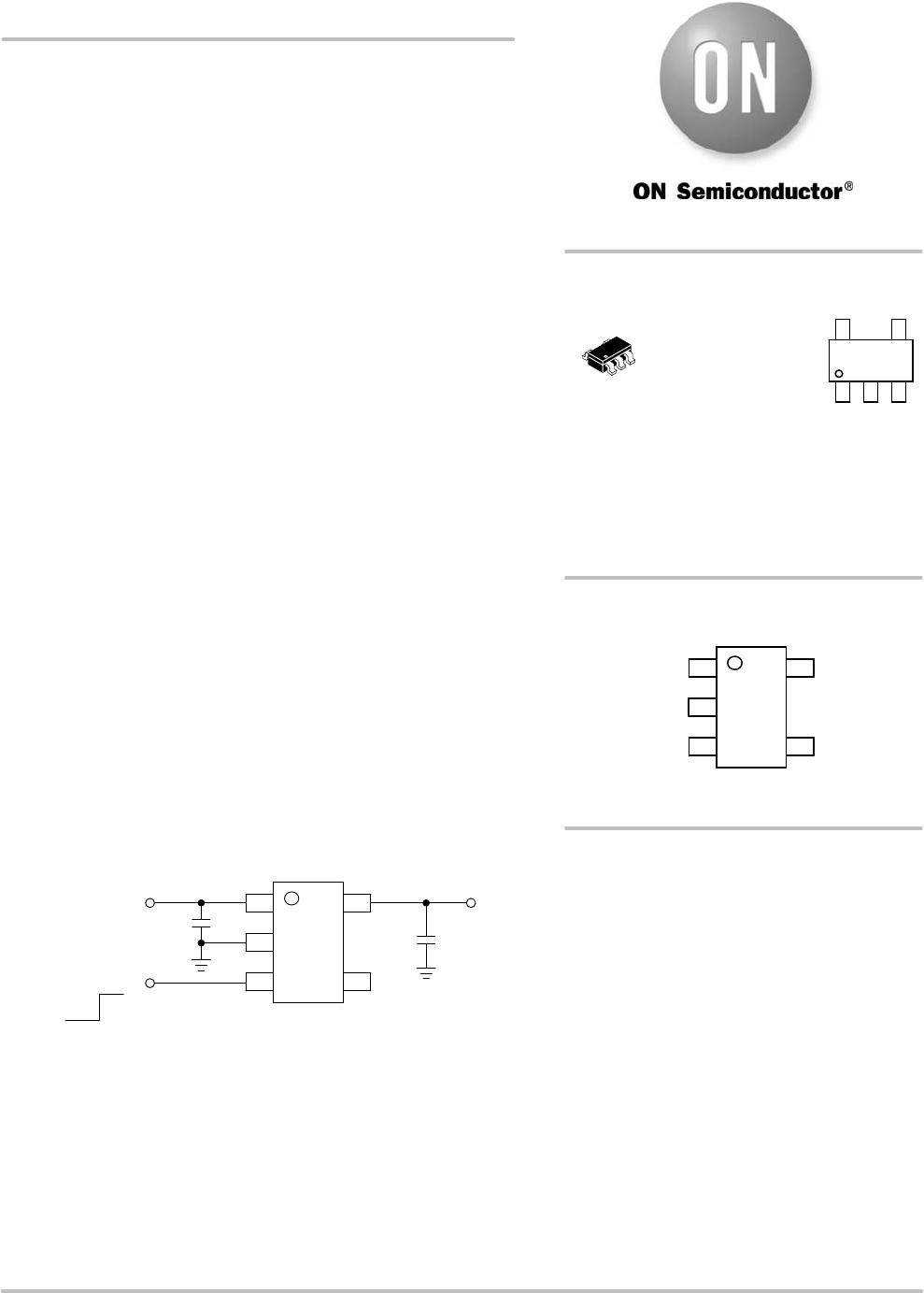
Figure 1. Typical Application Diagram
This device contains 86 active transistors
Vout
Battery or
Unregulated
Voltage
C
in
1 F
C
out
1 F
OFF
ON
1
2
3
5
4
+
+
See detailed ordering and shipping information in the package
dimensions section on page 7 of this data sheet.
ORDERING INFORMATION
TSOP5
(SOT235, SC595)
SN SUFFIX
CASE 483
PIN CONNECTIONS
1
3
N/C
V
in
2Gnd
Enable
4
V
out
5
(Top View)
MARKING
DIAGRAM
http://onsemi.com
(Note: Microdot may be in either location)
1
5
1
5
xxx AYWG
G
xxx = Specific Device Code
A = Assembly Location
Y = Year
W = Work Week
G = PbFree Package
NCP699
http://onsemi.com
2
PIN FUNCTION DESCRIPTION
Pin No. Pin Name Description
1 Vin Positive power supply input voltage.
2 Gnd Power supply ground.
3 Enable This input is used to place the device into lowpower standby. When this input is pulled low, the device is
disabled. If this function is not used, Enable should be connected to Vin.
4 N/C No internal connection.
5 Vout Regulated output voltage.
MAXIMUM RATINGS
Rating Symbol Value Unit
Input Voltage V
in
2.1 to 6.0 V
Enable Voltage Enable 0.3 to V
in
+0.3 V
Output Voltage V
out
0.3 to V
in
+0.3 V
Power Dissipation P
D
Internally Limited W
Operating Junction Temperature T
J
+150 °C
Maximum Junction Temperature T
J(max)
+150 °C
Operating Ambient Temperature T
A
40 to +85 °C
Storage Temperature T
stg
55 to +150 °C
Stresses exceeding Maximum Ratings may damage the device. Maximum Ratings are stress ratings only. Functional operation above the
Recommended Operating Conditions is not implied. Extended exposure to stresses above the Recommended Operating Conditions may affect
device reliability.
1. This device series contains ESD protection and exceeds the following tests:
Human Body Model 2000 V per MILSTD883, Method 3015
Machine Model Method 200 V
2. Latchup capability (85°C) "200 mA DC with trigger voltage.
THERMAL CHARACTERISTICS
Rating Symbol Test Conditions Typical Value Unit
JunctiontoAmbient
R
JA
1 oz Copper Thickness, 100 mm
2
250 °C/W
PSIJLead 2
JL2
1 oz Copper Thickness, 100 mm
2
68 °C/W
NOTE: Single component mounted on an 80 x 80 x 1.5 mm FR4 PCB with stated copper head spreading area. Using the following
boundary conditions as stated in EIA/JESD 511, 2, 3, 7, 12.
NCP699
http://onsemi.com
3
ELECTRICAL CHARACTERISTICS (V
in
= V
out(nom.)
+ 1.0 V, V
enable
= V
in
, C
in
= 1.0 F, C
out
= 1.0 F, T
A
= 25°C,
unless otherwise noted.)
Characteristic
Symbol Min Typ Max Unit
Output Voltage (I
out
= 10 mA, T
A
= 40°C to 85°C)
1.3 V
1.4 V
1.5 V
1.8 V
2.5 V
2.8 V
2.9 V
3.0 V
3.1 V
3.3 V
3.4 V
4.5 V
5.0 V
V
out
1.261
1.358
1.455
1.746
2.425
2.716
2.813
2.910
3.007
3.201
3.298
4.365
4.850
1.3
1.4
1.5
1.8
2.5
2.8
2.9
3.0
3.1
3.3
3.4
4.5
5.0
1.339
1.442
1.545
1.854
2.575
2.884
2.987
3.090
3.193
3.399
3.502
4.635
5.150
V
Line Regulation (I
out
= 10 mA)
1.3 V4.4 V (V
in
= V
out(nom.)
+ 1.0 V to 6.0 V)
4.5 V5.0 V (V
in
= 5.5 V to 6.0 V)
Reg
line
1.0
1.0
3.0
3.0
mV/V
Load Regulation (I
out
= 1.0 mA to 150 mA) Reg
load
0.3 0.8 mV/mA
Output Current Limit
1.3 V3.9 V (V
in
= V
out(nom.)
+ 2.0 V)
4.0 V5.0 V (V
in
= 6.0 V)
I
o(nom.)
150
150
240
240
mA
Dropout Voltage (I
out
= 150 mA,
Measured at V
out
= V
out(nom)
3.0%)
1.3 V
1.4 V
1.5 V
1.8 V
2.5 V
2.8 V
2.9 V
3.0 V
3.1 V
3.3 V
3.4 V
4.5 V 5.0 V
V
in
V
out
800
750
690
570
400
360
350
340
330
320
300
240
900
850
750
620
450
420
420
400
400
360
360
300
mV
Disable Current (T
A
= 40°C to 85°C)
(Enable Input = 0 V)
DIS
0.03 1.0
A
Ground Current (T
A
= 40°C to 85°C)
(Enable Input = V
in
, I
out
= 1.0 mA to I
o(nom.)
)
I
GND
40 90
A
Output Short Circuit Current (V
out
= 0 V)
1.3 V3.9 V (V
in
= V
out(nom.)
+ 2.0 V)
4.0 V5.0 V (V
in
= 6.0 V)
I
out(max)
150
150
300
300
600
600
mA
Output Voltage Noise (f = 100 Hz to 100 kHz)
I
out
= 30 mA, C
out
= 1 F
V
n
100
Vrms
Ripple Rejection
(f = 120 Hz, 15 mA)
(f = 1.0 kHz, 15 mA)
RR
55
50
dB
Enable Input Threshold Voltage (T
A
= 40°C to 85°C)
(Voltage Increasing, Output Turns On, Logic High)
(Voltage Decreasing, Output Turns Off, Logic Low)
V
th(en)
0.95
0.3
V
Output Voltage Temperature Coefficient T
C
"100 ppm/°C
3. Maximum package power dissipation limits must be observed.
PD +
T
J(max)
*T
A
R
JA
4. Low duty cycle pulse techniques are used during testing to maintain the junction temperature as close to ambient as possible.

NCP699SN34T1G

Mfr. #:
Manufacturer:
ON Semiconductor
Description:
LDO Voltage Regulators 150mA 3.4V CMOS LDO
Lifecycle:
New from this manufacturer.
Delivery:
DHL FedEx Ups TNT EMS
Payment:
T/T Paypal Visa MoneyGram Western Union