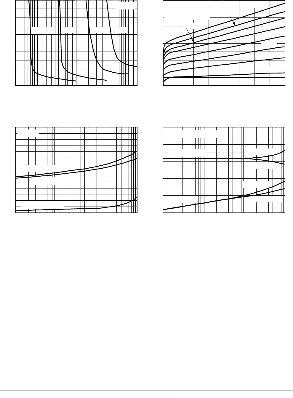
MMBT5087L
www.onsemi.com
6
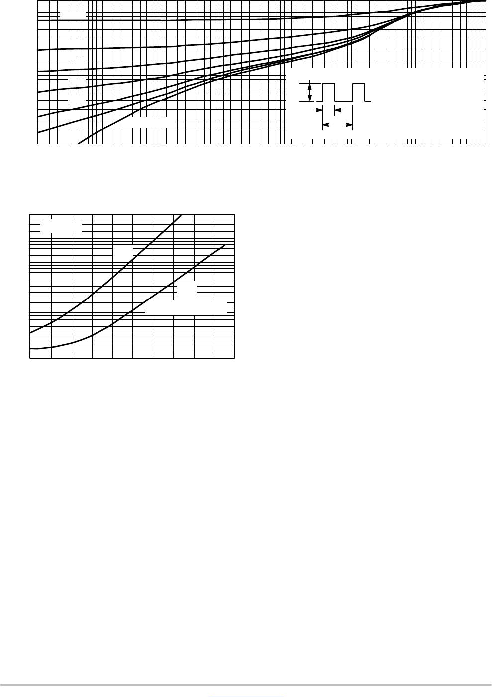
Figure 14. Thermal Response
t, TIME (ms)
1.0
0.01
r(t) TRANSIENT THERMAL RESISTANCE
(NORMALIZED)
0.01
0.02
0.03
0.05
0.07
0.1
0.2
0.3
0.5
0.7
0.02 0.05 0.1 0.2 0.5 1.0 2.0 5.0 10 20 50 100 200 500 1.0k 2.0k 5.0k 10k 20k
50k
100k
D = 0.5
0.2
0.1
0.05
0.02
0.01
SINGLE PULSE
DUTY CYCLE, D = t
1
/t
2
D CURVES APPLY FOR POWER
PULSE TRAIN SHOWN
READ TIME AT t
1
(SEE AN569/D)
Z
q
JA(t)
= r(t) • R
q
JA
T
J(pk)
− T
A
= P
(pk)
Z
q
JA(t)
t
1
t
2
P
(pk)
FIGURE 16
T
J
, JUNCTION TEMPERATURE (°C)
10
4
-4
0
I
C
, COLLECTOR CURRENT (nA)
Figure 15. Typical Collector Leakage Current
DESIGN NOTE: USE OF THERMAL RESPONSE DATA
A train of periodical power pulses can be represented by
the model as shown in Figure 16. Using the model and the
device thermal response the normalized effective transient
thermal resistance of Figure 14 was calculated for various
duty cycles.
To find Z
q
JA(t)
, multiply the value obtained from Figure
14 by the steady state value R
q
JA
.
Example:
Dissipating 2.0 watts peak under the following conditions:
t
1
= 1.0 ms, t
2
= 5.0 ms (D = 0.2)
Using Figure 14 at a pulse width of 1.0 ms and D = 0.2, the
reading of r(t) is 0.22.
The peak rise in junction temperature is therefore
DT = r(t) x P
(pk)
x R
q
JA
= 0.22 x 2.0 x 200 = 88°C.
For more information, see ON Semiconductor Application
Note AN569/D, available from the Literature Distribution
Center or on our website at www.onsemi.com.
10
-2
10
-1
10
0
10
1
10
2
10
3
-2
0
0 + 20 + 40 + 60 + 80 + 100 + 120 + 140 + 160
V
CC
= 30 V
I
CEO
I
CBO
AND
I
CEX
@ V
BE(off)
= 3.0 V