SiHB25N50E
www.vishay.com
Vishay Siliconix
S15-0493-Rev. A, 16-Mar-15
1
Document Number: 91646
For technical questions, contact: hvm@vishay.com
THIS DOCUMENT IS SUBJECT TO CHANGE WITHOUT NOTICE. THE PRODUCTS DESCRIBED HEREIN AND THIS DOCUMENT
ARE SUBJECT TO SPECIFIC DISCLAIMERS, SET FORTH AT www.vishay.com/doc?91000
E Series Power MOSFET
FEATURES
• Low figure-of-merit (FOM): R
on
x Q
g
• Low input capacitance (C
iss
)
• Reduced switching and conduction losses
• Low gate charge (Q
g
)
• Avalanche energy rated (UIS)
• Material categorization: for definitions of compliance
please see www.vishay.com/doc?99912
APPLICATONS
• Hard switched topologies
• Power factor correction power supplies (PFC)
• Switch mode power supplies (SMPS)
•Computing
- PC silver box / ATX power supplies
• Lighting
- Two stage LED lighting
Notes
a. Repetitive rating; pulse width limited by maximum junction temperature.
b. V
DD
= 50 V, starting T
J
= 25 °C, L = 28.2 mH, R
g
= 25 Ω, I
AS
= 4.4 A.
c. 1.6 mm from case.
d. I
SD
≤ I
D
, dI/dt = 100 A/μs, starting T
J
= 25 °C.
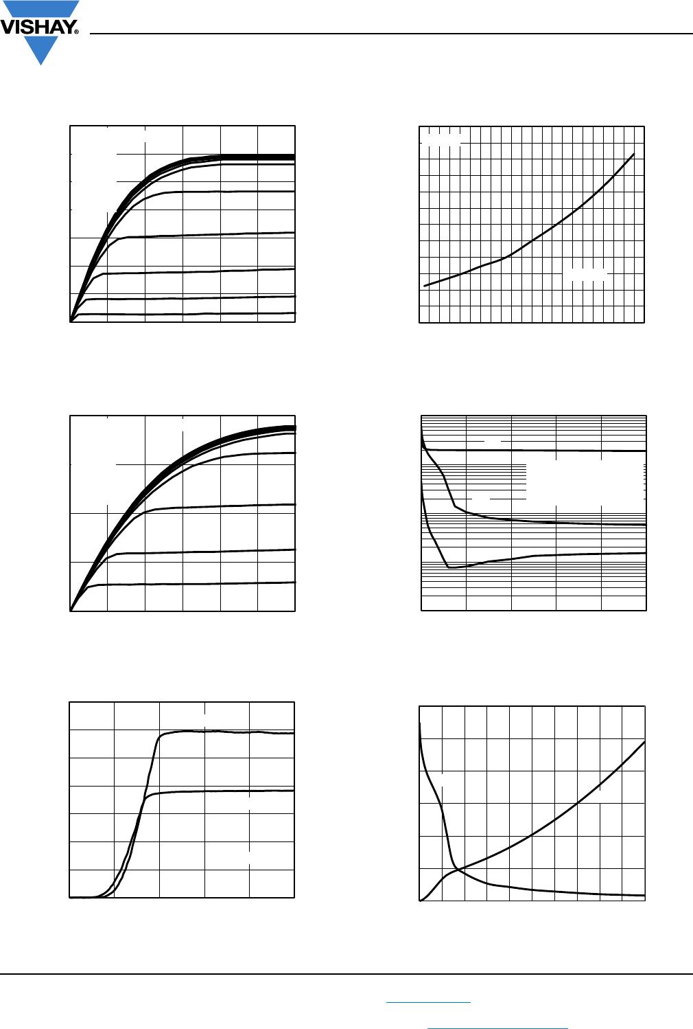
PRODUCT SUMMARY
V
DS
(V) at T
J
max. 550
R
DS(on)
max. at 25 °C (Ω)V
GS
= 10 V 0.145
Q
g
(Max.) (nC) 86
Q
gs
(nC) 14
Q
gd
(nC) 25
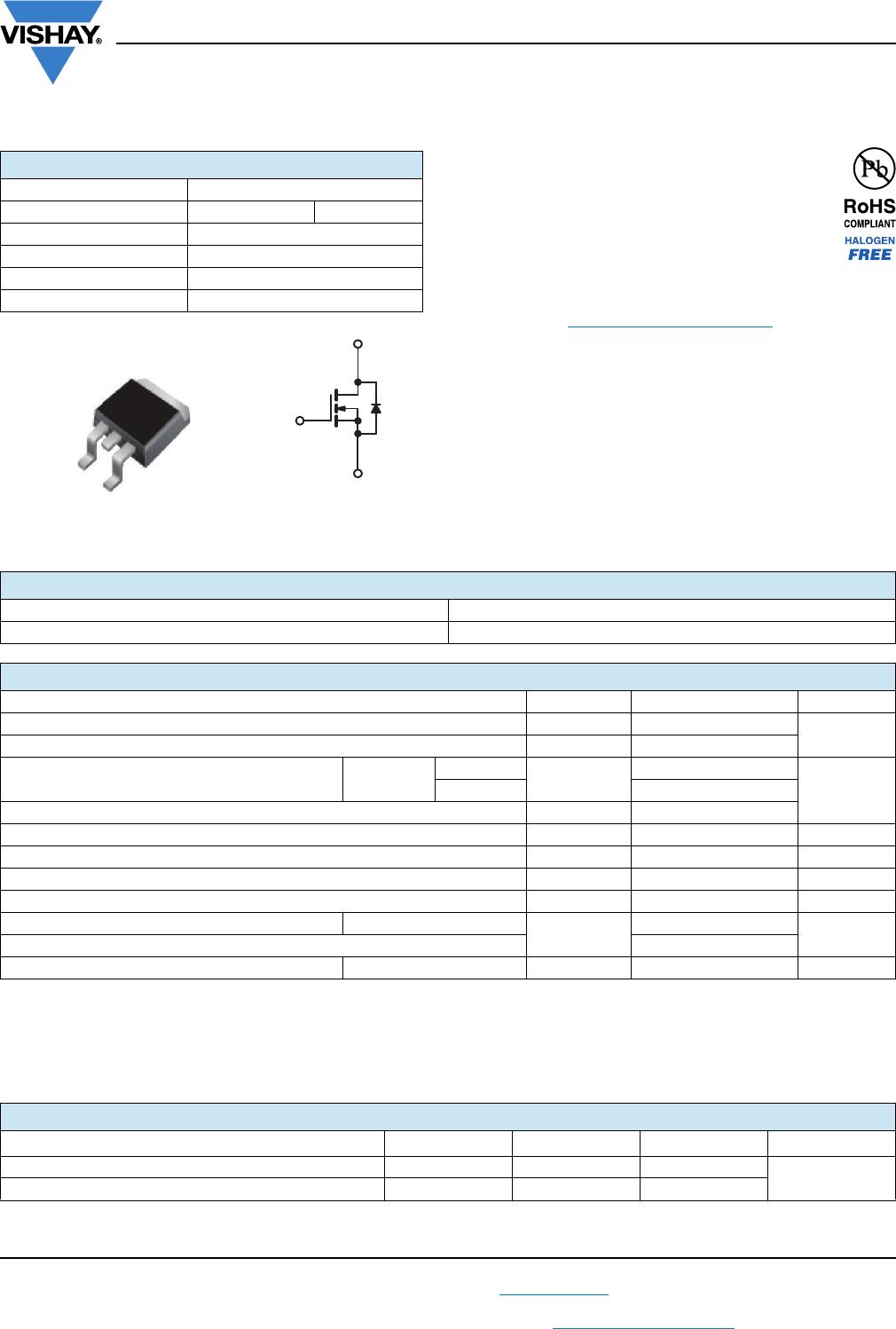
Configuration Single
D
2
PAK (TO-263)
G
D
S
ORDERING INFORMATION
Package D
2
PAK (TO-263)
Lead (Pb)-free and Halogen-free SiHB25N50E-GE3
ABSOLUTE MAXIMUM RATINGS (T
C
= 25 °C, unless otherwise noted)
PARAMETER SYMBOL LIMIT UNIT
Drain-Source Voltage V
DS
500
V
Gate-Source Voltage V
GS
± 30
Continuous Drain Current (T
J
= 150 °C) V
GS
at 10 V
T
C
= 25 °C
I
D
26
AT
C
= 100 °C 16
Pulsed Drain Current
a
I
DM
50
Linear Derating Factor 0.2 W/°C
Single Pulse Avalanche Energy
b
E
AS
273 mJ
Maximum Power Dissipation P
D
250 W
Operating Junction and Storage Temperature Range T
J
, T
stg
-55 to +150 °C
Drain-Source Voltage Slope V
DS
= 0 V to 80 % V
DS
dV/dt
65
V/ns
Reverse Diode dV/dt
d
25
Soldering Recommendations (Peak Temperature)
c
for 10 s 300 °C
THERMAL RESISTANCE RATINGS
PARAMETER SYMBOL TYP. MAX. UNIT
Maximum Junction-to-Ambient R
thJA
-62
°C/W
Maximum Junction-to-Case (Drain) R
thJC
-0.5