SIHB25N50E-GE3

SiHB25N50E
www.vishay.com
Vishay Siliconix
S15-0493-Rev. A, 16-Mar-15
4
Document Number: 91646
For technical questions, contact: hvm@vishay.com
THIS DOCUMENT IS SUBJECT TO CHANGE WITHOUT NOTICE. THE PRODUCTS DESCRIBED HEREIN AND THIS DOCUMENT
ARE SUBJECT TO SPECIFIC DISCLAIMERS, SET FORTH AT www.vishay.com/doc?91000
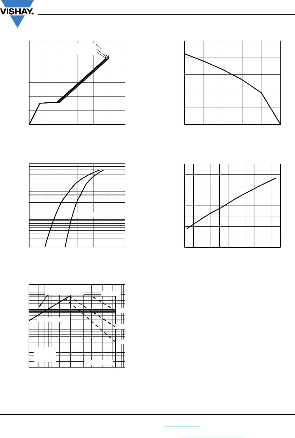
Fig. 7 - Typical Gate Charge vs. Gate-to-Source Voltage
Fig. 8 - Typical Source-Drain Diode Forward Voltage
Fig. 9 - Maximum Safe Operating Area
Fig. 10 - Maximum Drain Current vs. Case Temperature
Fig. 11 - Typical Drain-to-Source Voltage vs. Temperature
0
4
8
12
16
20
24
0 20406080100120
V
GS
, Gate-to-Source Voltage (V)
Q
g
, Total Gate Charge (nC)
V
DS
= 400 V
V
DS
= 250 V
V
DS
= 100 V
0.1
1
10
100
0.2 0.4 0.6 0.8 1.0 1.2 1.4
I
SD
, Reverse Drain Current (A)
V
SD
, Source-Drain Voltage (V)
T
J
= 150 °C
T
J
= 25 °C
V
GS
= 0 V
0.01
0.1
1
10
100
1101001000
I
D
, Drain Current (A)
V
DS
, Drain-to-Source Voltage (V)
* V
GS
> minimum V
GS
at which R
DS(on)
is specied
Limited by R
DS(on)
*
1 ms
I
DM
Limited
T
C
= 25 °C
T
J
= 150 °C
Single Pulse
BVDSS Limited
10 ms
100 μs
Operation in this Area
Limited by R
DS(on)
0
6
12
18
24
30
25 50 75 100 125 150
I
D
, Drain Current (A)
T
C
, Case Temperature (°C)
450
475
500
525
550
575
600
625
650
-60 -40 -20 0 20 40 60 80 100 120 140 160
V
DS
, Drain-to-Source Breakdown Voltage (V)
T
J
, Junction Temperature (°C)
I
D
= 250 μA
SiHB25N50E
www.vishay.com
Vishay Siliconix
S15-0493-Rev. A, 16-Mar-15
5
Document Number: 91646
For technical questions, contact: hvm@vishay.com
THIS DOCUMENT IS SUBJECT TO CHANGE WITHOUT NOTICE. THE PRODUCTS DESCRIBED HEREIN AND THIS DOCUMENT
ARE SUBJECT TO SPECIFIC DISCLAIMERS, SET FORTH AT www.vishay.com/doc?91000
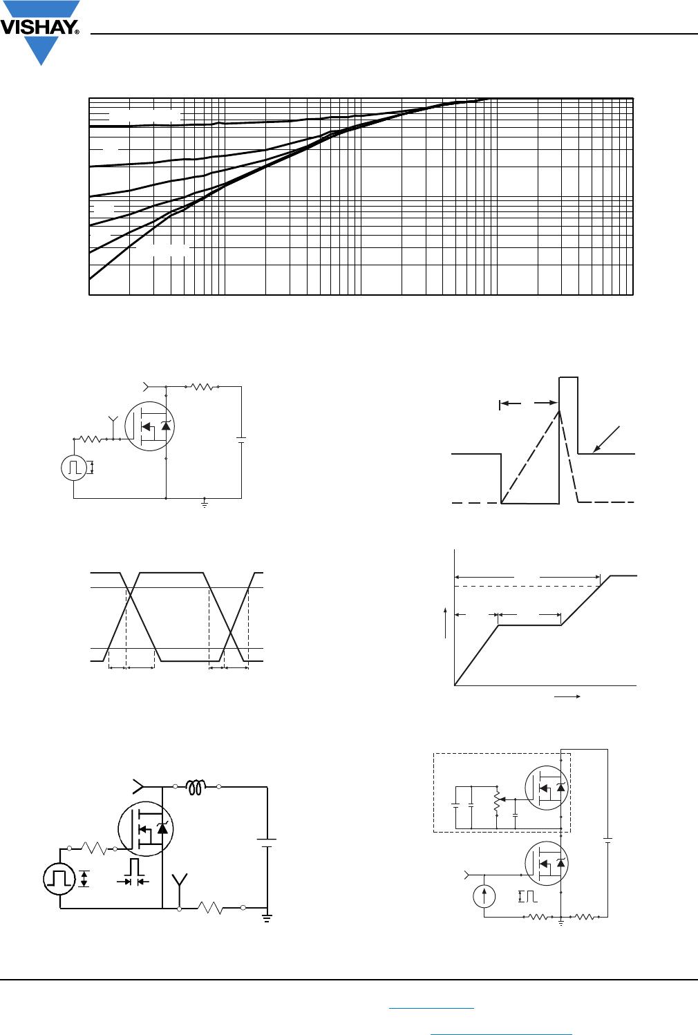
Fig. 12 - Normalized Thermal Transient Impedance, Junction-to-Case
Fig. 13 - Switching Time Test Circuit
Fig. 14 - Switching Time Waveforms
Fig. 15 - Unclamped Inductive Test Circuit
Fig. 16 - Unclamped Inductive Waveforms
Fig. 17 - Basic Gate Charge Waveform
Fig. 18 - Gate Charge Test Circuit
0.01
0.1
1
0.0001 0.001 0.01 0.1 1
Normalized Effective Transient
Thermal Impedance
Pulse Time (s)
Duty Cycle = 0.5
0.2
0.1
0.05
0.02
Single Pulse
V
DS
90 %
10 %
V
GS
t
d(on)
t
r
t
d(off)
t
f
R
G
I
AS
0.01 Ω
t
p
D.U.T
L
V
DS
+
-
V
DD
10 V
Vary t
p
to obtain
required I
AS
I
AS
V
DS
V
DD
V
DS
t
p
Q
GS
Q
GD
Q
G
V
G
Charge
10 V
D.U.T.
3 mA
V
GS
V
DS
I
G
I
D
0.3 µF
0.2 µF
50 kΩ
12 V
Current regulator
Current sampling resistors
Same type as D.U.T.
+
-
SiHB25N50E
www.vishay.com
Vishay Siliconix
S15-0493-Rev. A, 16-Mar-15
6
Document Number: 91646
For technical questions, contact: hvm@vishay.com
THIS DOCUMENT IS SUBJECT TO CHANGE WITHOUT NOTICE. THE PRODUCTS DESCRIBED HEREIN AND THIS DOCUMENT
ARE SUBJECT TO SPECIFIC DISCLAIMERS, SET FORTH AT www.vishay.com/doc?91000
Fig. 19 - For N-Channel
Vishay Siliconix maintains worldwide manufacturing capability. Products may be manufactured at one of several qualified locations. Reliability data for Silicon
Technology and Package Reliability represent a composite of all qualified locations. For related documents such as package/tape drawings, part marking, and
reliability data, see www.vishay.com/ppg?91646
.
P.W.
Period
dI/dt
Diode recovery
dV/dt
Ripple 5 %
Body diode forward drop
Re-applied
voltage
Reverse
recovery
current
Body diode forward
current
V
GS
= 10 V
a
I
SD
Driver gate drive
D.U.T. l
SD
waveform
D.U.T. V
DS
waveform
Inductor current
D =
P.W.
Period
+
-
+
+
+
-
-
-
Peak Diode Recovery dV/dt Test Circuit
V
DD
dV/dt controlled by R
g
Driver same type as D.U.T.
I
SD
controlled by duty factor “D”
D.U.T. - device under test
D.U.T.
Circuit layout considerations
Low stray inductance
Ground plane
Low leakage inductance
current transformer
R
g
Note
a. V
GS
= 5 V for logic level devices
V
DD
SIHB25N50E-GE3

Mfr. #:
Manufacturer:
Vishay / Siliconix
Description:
MOSFET 500V Vds 30V Vgs D2PAK (TO-263)
Lifecycle:
New from this manufacturer.
Delivery:
DHL FedEx Ups TNT EMS
Payment:
T/T Paypal Visa MoneyGram Western Union

Products related to this Datasheet