October 2009 Doc ID 6972 Rev 6 1/18
18
TS94x, TS94xA, TS94xB
Output rail-to-rail micropower operational amplifiers
Features
Rail-to-rail output voltage swing
Micropower consumption (1.2 µA)
Single supply operation (2.5 V to 10 V)
CMOS inputs
Ultra low input bias current (1 pA)
ESD protection (2 kV)
Latch-up immunity (class A)
Available in SOT23-5 micropackage
Applications
Battery-powered systems (alarm)
Portable communication systems (pagers)
Smoke/gas/fire detectors
Instrumentation and sensoring
PH meter
Description
The TS94x (single, dual and quad) series are
operational amplifiers characterized for 2.5 V to
10 V operation over a -40° C to +85° C
temperature range.
They exhibit excellent consumption -1.2 µA, while
featuring 10 kHz gain bandwidth product, 1.5 mA
output capability and output rail-to-rail operation
- 2.85 V typical at 3 V with R
L
=10 kΩ.
The TS94x op-amps are ideal for battery-powered
systems, where very low supply current and
output rail-to-rail are required. Their very low
- 1 pA typical input bias current and constant
supply current over supply voltage enhance the
devices’ performance near the end of the battery
charge or battery life.
Table 1. Device summary
Reference Selection on offset voltage
TS94x TS941, TS942, TS944
TS94xA TS941A, TS942A, TS944A
TS94xB TS941B, TS942B, TS944B
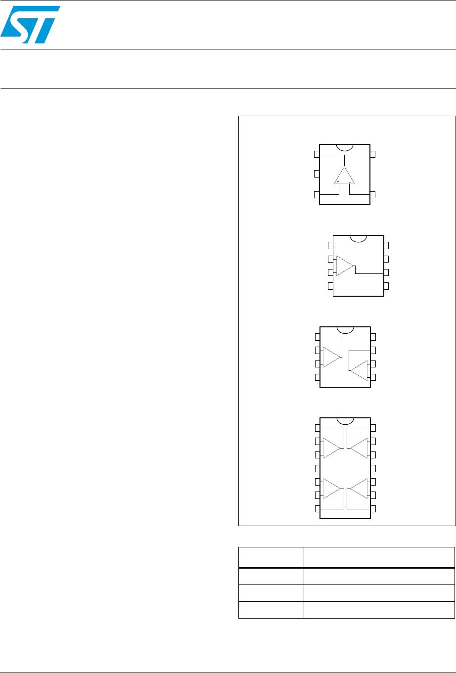
1
2
3
4
5
Inverting input
Non-inverting input
Output
V
DD
V
CC
1
2
3
4
5
6
7
8
-
+
Inverting Input 1
N.C.
Non-inverting Input 1
V
DD
V
CC
Output 2
N.C.
N.C.
Inverting Input 2
Non-inverting Input 2
Non-inverting Input 1
DD
V
1
2
3
4
8
5
6
7
9
10
11
12
13
14
CC
V
Output 3
Output 4
Non-inverting Input 4
Inverting Input 4
Non-inverting Input 3
Inverting Input 3
-
+
-
+
-
+
-
+
Output 1
Inverting Input 1
Output 2
1
2
3
45
6
7
8
-
+
-
+
Inverting Input 1
Output 1
Non-inverting Input 1
V
DD
V
CC
Output 2
Inverting Input 2
Non-inverting Input 2
TS941ILT
TS944ID-TS944IDT-TS944IPT
TS941ID-TS941IDT
TS942ID-TS942IDT-TS942IPT
www.st.com
Absolute maximum ratings and operating conditions TS94x, TS94xA, TS94xB
2/18 Doc ID 6972 Rev 6
1 Absolute maximum ratings and operating conditions
Table 2. Absolute maximum ratings
Symbol Parameter Value Unit
V
CC
Supply voltage
(1)
1. All voltage values, except differential voltage are with respect to network terminal.
12 V
V
id
Differential input voltage
(2)
2. Differential voltages are the non-inverting input terminal with respect to the inverting input terminal.
± V
CC
V
V
in
Input voltage range
(3)
3. The magnitude of input and output voltages must never exceed V
CC
+0.3 V.
V
DD
-0.3 to V
CC
+0.3 V
T
stg
Storage temperature range -65 to +150 °C
T
j
Maximum junction temperature 150 °C
R
thja
Thermal resistance junction to ambient
(4)
SOT23-5
SO-8
SO-14
TSSOP8
TSSOP14
4. Short-circuits can cause excessive heating and destructive dissipation. R
th
are typical values.
250
125
103
120
100
°C/W
R
thjc
Thermal resistance junction to case
(4)
SOT23-5
SO-8
SO-14
TSSOP8
TSSOP14
81
40
31
37
32
°C/W
ESD
HBM: human body model
(5)
5. Human body model: a 100 pF capacitor is charged to the specified voltage, then discharged through a
1.5 kΩ resistor between two pins of the device. This is done for all couples of connected pin combinations
while the other pins are floating.
2kV
MM: machine model
(6)
(TS941, TS942)
6. Machine model: a 200 pF capacitor is charged to the specified voltage, then discharged directly between
two pins of the device with no external series resistor (internal resistor < 5 Ω). This is done for all couples of
connected pin combinations while the other pins are floating.
200 V
CDM: charged device model
(7)
TS941 - TS944IDT
TS942 - TS944IPT
7. Charged device model: all pins and the package are charged together to the specified voltage and then
discharged directly to the ground through only one pin. This is done for all pins.
1.5
1
kV
Latch-up immunity 200 mA
Lead temperature (soldering, 10sec) 250 °C
TS94x, TS94xA, TS94xB Absolute maximum ratings and operating conditions
Doc ID 6972 Rev 6 3/18
Table 3. Operating conditions
Symbol Parameter Value Unit
V
CC
Supply voltage 2.5 to 10 V
V
icm
Common mode input voltage range V
DD
-0.2 to V
CC
-1.3 V
T
oper
Operating free air temperature range -40 to + 85 °C

TS942IDT

Mfr. #:
Manufacturer:
STMicroelectronics
Description:
Operational Amplifiers - Op Amps Dual Rail-to-Rail
Lifecycle:
New from this manufacturer.
Delivery:
DHL FedEx Ups TNT EMS
Payment:
T/T Paypal Visa MoneyGram Western Union