Electrical characteristics TS94x, TS94xA, TS94xB
4/18 Doc ID 6972 Rev 6
2 Electrical characteristics
Table 4. V
CC
= +2.5 V, V
DD
= 0 V, R
L
connected to V
CC
/2, T
amb
= 25° C
(unless otherwise specified)
Symbol Parameter Min. Typ. Max. Unit
V
io
Input offset voltage
TS941/2/4
TS941/2/4A
TS941/2/4B
10
5
2
mV
ΔV
io
Input offset voltage drift 7 µV/°C
I
io
Input offset current
(1)
1. Maximum values include unavoidable inaccuracies of the industrial tests.
1 100 pA
I
ib
Input bias current
(1)
1 150 pA
CMR Common mode rejection ratio 60 85 dB
SVR Supply voltage rejection ratio 50 78 dB
A
vd
Large signal voltage gain
V
O
= 2 V
pp
, R
L
= 1 MΩ
100 dB
V
OH
High level output voltage
V
ID
= 100 mV, R
L
= 1 MΩ
R
L
= 10 kΩ
2.45
2.3
2.49
2.4
V
V
OL
Low level output voltage
V
ID
= -100 mV, R
L
= 1 MΩ
R
L
= 10 kΩ
1
100
5
200
mV
I
o
Output source current
V
ID
= 100 mV, V
O
= V
DD
Output sink current
V
ID
= -100 mV, V
O
= V
CC
350
280
650
500
µA
I
CC
Supply current (per amplifier), A
VCL
= 1, no load 1.2 1.8 µA
GBP Gain bandwidth product, R
L
= 1 MΩ, C
L
= 50 pF 10 kHz
SR Slew rate, R
L
= 1 MΩ, C
L
= 50 pF 3 4.5 V/ms
φm Phase margin, C
L
= 50 pF 65 Degrees
TS94x, TS94xA, TS94xB Electrical characteristics
Doc ID 6972 Rev 6 5/18
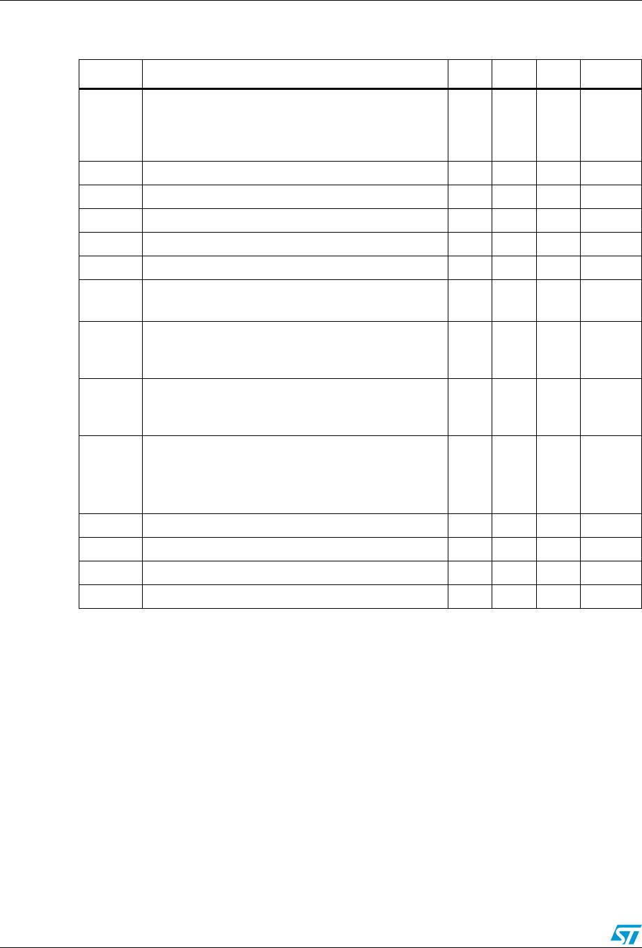
Table 5. V
CC
= +3 V, V
DD
= 0 V, R
L
connected to V
CC
/2,T
amb
= 25° C
(unless otherwise specified)
(1)
1. All electrical values are guaranteed with correlation measurements at 2.5 V and 5 V.
Symbol Parameter Min. Typ. Max. Unit
V
io
Input offset voltage
TS941/2/4
TS941/2/4A
TS941/2/4B
10
5
2
mV
ΔV
io
Input offset voltage drift 7 µV/°C
I
io
Input offset current
(2)
2. Maximum values include unavoidable inaccuracies of the industrial tests.
1 100 pA
I
ib
Input bias current
(2)
1 150 pA
CMR Common mode rejection ratio 60 85 dB
SVR Supply voltage rejection ratio 50 85 dB
A
vd
Large signal voltage gain
V
O
= 2 V
pp
,R
L
= 1 MΩ
100 dB
V
OH
High level output voltage
V
ID
= 100 mV, R
L
= 1 MΩ
R
L
= 10 kΩ
2.9
2.8
2.99
2.85
V
V
OL
Low level output voltage
V
ID
= -100 mV, R
L
= 1 MΩ
R
L
= 10 kΩ
1
100
5
200
mV
I
o
Output source current
V
ID
= 100 mV, V
O
= V
DD
Output sink current
V
ID
= -100 mV, V
O
= V
CC
680
650
1500
1300
µA
I
CC
Supply current (per amplifier), A
VCL
= 1, no load 1.2 1.8 µA
GBP Gain bandwidth product, R
L
= 1 MΩ, C
L
= 50 pF 10 kHz
SR Slew rate, R
L
= 1 MΩ, C
L
= 50 pF 3 4.5 V/ms
φm Phase margin, C
L
= 50 pF 65 Degrees
Electrical characteristics TS94x, TS94xA, TS94xB
6/18 Doc ID 6972 Rev 6
Table 6. V
CC
= +5 V, V
DD
= 0 V, R
L
connected to V
CC
/2, T
amb
= 25° C
(unless otherwise specified)
Symbol Parameter Min. Typ. Max. Unit
V
io
Input offset voltage
TS941/2/4
TS941/2/4A
TS941/2/4B
10
5
2
mV
ΔV
io
Input offset voltage drift 7 µV/°C
I
io
Input offset current
(1)
1. Maximum values include unavoidable inaccuracies of the industrial tests.
1 100 pA
I
ib
Input bias current
(1)
1 150 pA
CMR Common mode rejection ratio 60 85 dB
SVR Supply voltage rejection ratio 50 85 dB
A
vd
Large signal voltage gain
V
O
= 2 V
pp
, R
L
= 1 MΩ
100 dB
V
OH
High level output voltage
V
ID
= 100 mV, R
L
= 1 MΩ
R
L
= 10 kΩ
4.9
4.8
4.99
4.85
V
V
OL
Low level output voltage
V
ID
= -100 mV, R
L
= 1 MΩ
R
L
= 10 kΩ
1
100
5
150
mV
I
o
Output source current
V
ID
= 100 mV, V
O
= V
DD
Output sink current
V
ID
= -100 mV, V
O
= V
CC
3
3.7
4.5
5
mA
I
CC
Supply current (per amplifier), A
VCL
= 1, no load 1.2 1.85 µA
GBP Gain bandwidth product, R
L
= 1 MΩ, C
L
= 50 pF 10 kHz
SR Slew rate, R
L
= 1 MΩ, C
L
= 50 pF 3 4.5 V/ms
φm Phase margin, C
L
= 50 pF 65 Degrees

TS942IDT

Mfr. #:
Manufacturer:
STMicroelectronics
Description:
Operational Amplifiers - Op Amps Dual Rail-to-Rail
Lifecycle:
New from this manufacturer.
Delivery:
DHL FedEx Ups TNT EMS
Payment:
T/T Paypal Visa MoneyGram Western Union