AD8345
Rev. B | Page 12 of 20
BASIC CONNECTIONS
16
15
14
13
12
11
10
9
1
2
3
4
5
6
7
8
AD8345
QBBP
QBBN
COM3
COM3
VPS2
VOUT
COM2
COM3
IBBP
IBBN
COM3
COM1
LOIN
LOIP
VPS1
ENBL
IP
1
T1
ETC1-1-13
2
34
5
LO
R1
50Ω
C6
1000pF
C7
1000pF
IN
C3
1000pF
C4
0.01μF
+V
S
QP
QN
C1
1000pF
C2
0.01μF
+V
S
VOUT
C5
1000pF
00932-028
Figure 28. Basic Connections
The basic connections for operating the AD8345 are shown in
Figure 28. A single power supply of between 2.7 V and 5.5 V is
applied to the VPS1 pin and the VPS2 pin. A pair of ESD
protection diodes is connected internally between the VPS1 pin
and the VPS2 pin so these must be tied to the same potential.
Both pins should be individually decoupled using 1000 pF and
0.01 μF capacitors, located as close as possible to the device. For
normal operation, the enable pin (ENBL) must be pulled high.
The turn-on threshold for ENBL is V
S
/2. COM1 to COM3
should all be tied to the same low impedance ground plane.
LO DRIVE
In Figure 28, a 50 Ω resistor to ground combines with the
devices high input impedance to provide an overall input
impedance of approximately 50 Ω (see
Figure 19 for a plot of
LO port input impedance). For maximum LO suppression at
the output, a differential LO drive is recommended. In
Figure 28, this is achieved using a balun (M/A-COM part
number ETC1-1-13).
The outputs of the balun are ac-coupled to the LO inputs, which
have a bias level of approximately 1.8 V dc. An LO drive level of
−2 dBm is recommended for lowest output noise. Higher levels
degrade linearity while lower levels tend to increase the noise
floor slightly. For example, reducing the LO power from −2 dBm
to −10 dBm increases the noise floor by approximately 0.3 dB
(see
Figure 21).
The LO input pins can be driven single-ended at the expense of
slightly higher LO leakage. LOIN is ac-coupled to ground using
a capacitor and LOIP is driven through a coupling capacitor
from a (single-ended) 50 Ω source. (This scheme could also be
reversed with the drive signal being applied to LOIN.)
LO FREQUENCY RANGE
The frequency range on the LO input is limited by the internal
quadrature phase splitter. The phase splitter generates drive
signals for the internal mixers which are 90° out of phase
relative to one another.
Outside of the specified LO frequency range of 140 MHz to 1 GHz,
this quadrature accuracy degrades, resulting in decreased sideband
suppression. See
Figure 11 for a plot of sideband suppression vs.
LO frequency from 250 MHz to 1 GHz.
Figure 29 shows the
sideband suppression of a typical device from 70 MHz to 300 MHz.
LO FREQUENCY (MHz)
40
SIDEBAND SUPPRESSION (dBc)
60 80 100 120 140 160 180 200 220 240 260 280 300
–50
–45
–40
–35
–30
–25
–20
–15
–10
–5
V
S
= 5V, DIFFERENTIAL INPUT = 1.2V
00932-029
0
Figure 29. Typical Lower Frequency Sideband Suppression Performance
AD8345
Rev. B | Page 13 of 20
BASEBAND I AND Q CHANNEL DRIVE
The I channel and Q channel baseband inputs should be driven
differentially. This is convenient as most modern high-speed
DACs have differential outputs. For optimal performance at
V
S
= 5 V, the drive signal should be a 1.2 V p-p differential
signal with a bias level of 0.7 V; that is, each input should swing
from 0.4 V to 1 V. If the AD8345 is being run on a lower supply
voltage, then the peak-to-peak voltage on the I and Q channel
inputs must be reduced to avoid input clipping. For example, at
a supply voltage of 2.7 V, a 200 mV p-p differential drive is
recommended. This results in a corresponding reduction in
output power (see
Figure 3). The I and Q inputs have a large
input bandwidth of approximately 80 MHz. At lower baseband
input levels, the input bandwidth increases (see
Figure 4).
If the baseband signal has a high peak-to-average ratio (such as
CDMA or WCDMA), then the rms signal strength must be
backed off from this peak level in order to prevent clipping of
the signal peaks.
Clipping of signal peaks tends to increase signal leakage into
adjacent channels. Backing off the I and Q signal strength, in
the manner recommended, reduces the output power by a
corresponding amount. This also applies to multicarrier
applications where the per-carrier output power is lower by
3 dB for each doubling of the number of output carriers.
The I and Q inputs have high input impedances because they
connect directly to the bases of PNP transistors. If a dc-coupled
filter is being used between a DAC and the modulator inputs,
then the filter must be terminated with the appropriate
resistance. If the filter is differential, then the termination
resistor should be connected across the I and Q differential
inputs.
REDUCTION OF LO LEAKAGE
Because the I and Q signals are being effectively multiplied with
the LO, any internal offset voltages on these inputs result in
leakage of the LO. The nominal LO leakage of −42 dBm, which
results from these internal offset voltages, can be reduced further
by applying offset compensation voltages on the I and Q inputs.
(Note that LO feedthrough is reduced by varying the differential
offset voltages on the I and Q inputs, not by varying the nominal
bias level of 0.7 V.) The reduction is easily accomplished by
programming (and then storing) the appropriate DAC offset
code. This does, however, require dc coupling the path from the
DAC to the I and Q inputs. (DC coupling is also advantageous
from the perspective of I and Q input biasing if the DAC is
capable of delivering a bias level of 0.7 V.)
The procedure for reducing the LO feedthrough is simple. In
order to isolate the LO in the output spectrum, a single
sideband configuration is recommended (set I and Q signals to
sine and cosine waves at, for example, 100 kHz; set LO to
F
RF
− 100 kHz). An offset voltage is applied from the I DAC
until the LO leakage reaches a trough. With this offset level
held, an offset voltage is applied to the Q DAC until a (lower)
trough is reached.
LO leakage compensation holds up well over temperature.
Figure 10 shows the effect of temperature on LO leakage after
compensation at ambient.
Compensated LO leakage degrades somewhat as the frequency
is moved away from the frequency at which the compensation
was performed. This is due to the effects of LO to RF output
leakage, which is not a result of offsets on the I and Q inputs.
SINGLE-ENDED I AND Q DRIVE
Where only single-ended I and Q signals are available, a
differential amplifier such as the AD8132 or AD8138 can be
used to generate the required differential drive signal for the
AD8345.
Although most DACs have differential outputs, using a single-
ended, low-pass filter between the dual DAC and the I and Q
inputs can be more desirable from the perspective of
component count and cost. As a result, the output signal from
the filter must be converted back to differential mode and
possibly be rebiased to 0.7 V common mode.
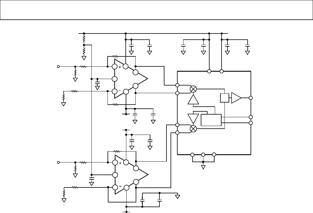
Figure 30 shows a circuit that converts a ground-referenced,
single-ended signal to a differential signal and adds the required
0.7 V bias voltage. Two AD8132 differential op amps configured
for unity gain are used. With a 50 Ω input impedance, this
circuit is configured to accept a signal from a 50 Ω source (for
example, a low-pass filter). The input impedance can be easily
changed by replacing the 49.9 Ω shunt resistor (and the
corresponding 24.9 Ω resistor on the inverting input) with the
appropriate value. The required dc-bias level is conveniently
added to the signal by applying 0.7 V to the V
OCM
pins of the
differential amplifiers.
Differential amplifiers, such as the AD8132 and AD8138, can
also be used to implement active filters. For more information
on this topic, refer to the data sheets of these devices.
AD8345
Rev. B | Page 14 of 20
8
2
1
6
4
5
8
2
1
6
4
5
+5V
10kΩ
1.5kΩ
AD8132
PHASE
SPLITTER
VOUT
IBBP
Σ
IBBN
QBBP
QBBN
AD8345
LOIP
LOIN
VPS1 VPS2
0.01μF
1000pF
0.1μF10μF
+5V
+
+
348Ω
348Ω
348Ω
0.1μF
348Ω
49.9Ω
348Ω
24.9Ω
348Ω
AD8132
0.1μF
10μF
–5V
10μF0.1μF
+
COM1 COM2 COM3
–5V
3
3
0.1μF
348Ω
24.9Ω
348Ω
49.9Ω
I
IN
Q
IN
0.1μF10μF
+
0.01μF
1000pF
00932-030
Figure 30. Single-Ended 1Q Drive Circuit
Note that this circuit assumes that the single-ended I and Q
signals are ground-referenced. Any differential dc-offsets result
in increased LO leakage at the output of the AD8345.
It is possible to drive the baseband inputs with a single-ended
signal biased to 0.7 V, with the unused inputs being biased to a
dc level of 0.7 V. However, this mode of operation is not recom-
mended because any dc level difference between the bias level
of the drive signal and the dc level on the unused input
(including the effect of temperature drift) results in increased
LO leakage. In addition, the maximum output power is reduced
by 6 dB.
RF OUTPUT
The RF output is designed to drive a 50 Ω load but should be ac
coupled as shown in
Figure 28. If the I and Q inputs are driven
in quadrature by 1.2 V p-p signals, then the resulting output
power is approximately −1 dBm (see
Figure 3). The RF output
impedance is very close to 50 Ω. As a result, no additional
matching circuitry is required if the output is driving a 50 Ω
load.
APPLICATION WITH TxDAC®
Figure 31 shows the AD8345 driven by the AD9761 TxDAC.
(Any of the devices in the Analog Devices’ TxDAC family can
also be used in this application.)
The I and Q DACs generate differential output currents of 0 mA
to 10 mA and 10 mA to 0 mA, respectively. The combination of
140 Ω resistors shunted to ground off each DAC output, along
with 210 Ω resistors shunted between each differential DAC
pair, produces a baseband signal into the AD8345 I and Q
inputs that has a differential peak-to-peak swing of 1.2 V with a
dc common-mode bias of 700 mV.

AD8345AREZ

Mfr. #:
Manufacturer:
Analog Devices Inc.
Description:
Modulator / Demodulator 140MHz TO 1000MHz Quadrature
Lifecycle:
New from this manufacturer.
Delivery:
DHL FedEx Ups TNT EMS
Payment:
T/T Paypal Visa MoneyGram Western Union