AD8345
Rev. B | Page 15 of 20
210Ω
140Ω140Ω
PHASE
SPLITTER
VOUT
IBBP
IBBN
QBBP
QBBN
AD8345
LOIP
LOIN
VPS1 VPS2
IOUTB
IOUTA
2⋅
2⋅
LATCH
"Q"
"Q"
DAC
"I"
DAC
LATCH
"I"
QOUTA
0.1μF
R
SET
2kΩ
REFIOFS ADJ
SLEEP
SELECT
WRITE
CLOCK
AD9761
MUX
CONTROL
AVDDDVDD DCOM
QOUTB
DAC
DATA
INPUTS
210Ω
140Ω140Ω
Σ
00932-031
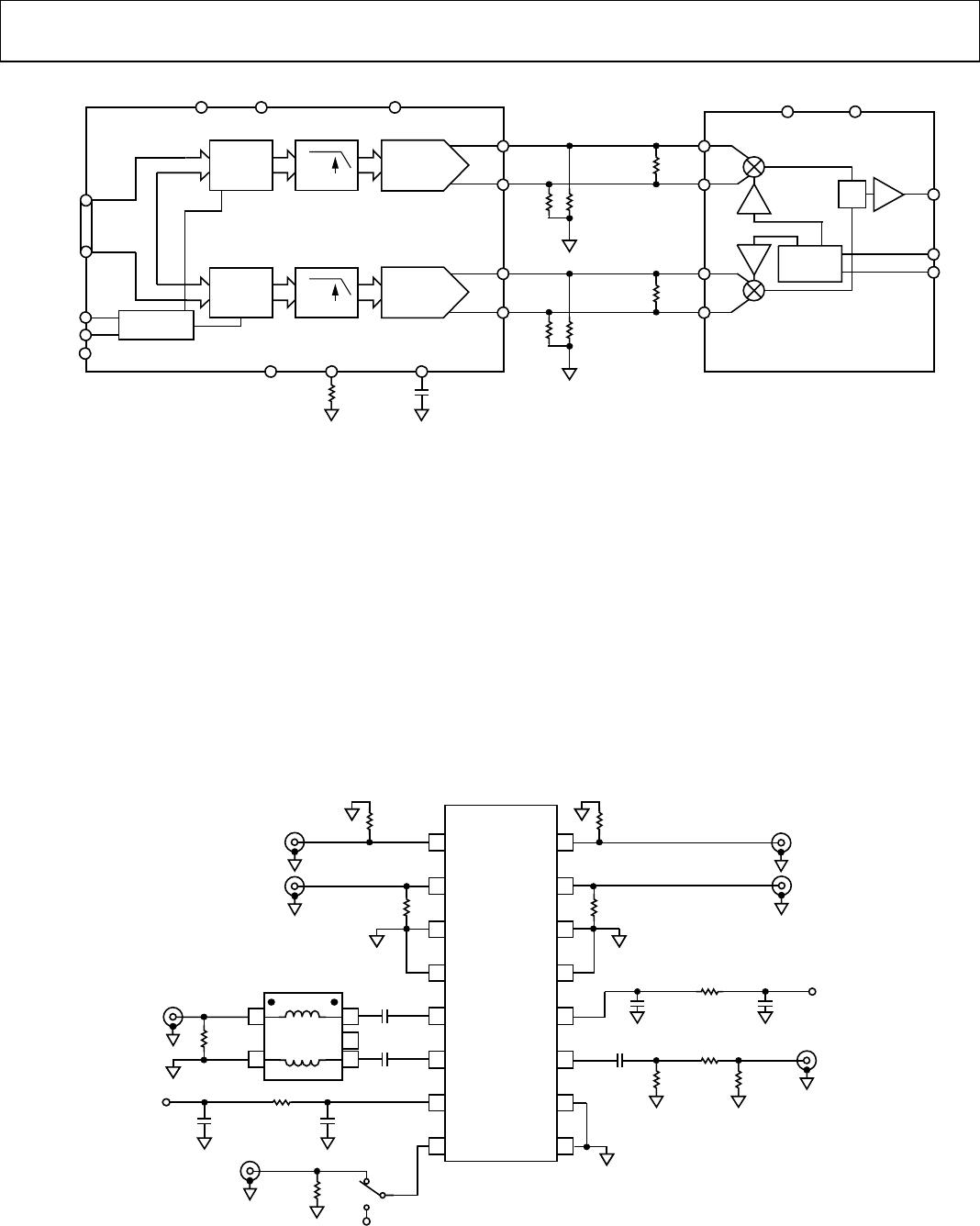
Figure 31. AD8345/TxDAC Interface
SOLDERING INFORMATION
The AD8345 is packaged in a 16-lead TSSOP_EP package. For
optimum thermal conductivity, the exposed pad can be
soldered to the exposed metal of a ground plane. This results in
a junction-to-air thermal impedance (θ
JA
) of 30°C/W. However,
soldering is not necessary for safe operation. If the exposed pad
is not soldered down, then the θ
JA
is equal to 95°C/W.
EVALUATION BOARD
Figure 32 shows the schematic of the AD8345 evaluation board.
Note that uninstalled components are marked as open. This is a
4-layer board, with the two center layers used as ground plane,
and top and bottom layers used as signal and power planes.
The board is powered by a single supply (V
S
) in the range 2.7 V
to 5.5 V. The power supply is decoupled by 0.01 μF and 1000 pF
capacitors. The circuit closely follows the basic connection
schematic with SW1 in Position B. If SW1 is in Position A, the
enable pin (ENBL) is pulled to ground by a 10 kΩ resistor, and
the device is in its power-down mode.
All connectors are SMA-type. The I and Q inputs are dc-coupled to
allow a direct connection to a dual DAC with differential outputs.
Resistor pads are provided in case termination at the I and Q inputs
is required. The local oscillator input (LO) is terminated to approxi-
mately 50 Ω with an external 50 Ω resistor to ground. A 1:1 wide-
band transformer (ETC1-1-13) provides a differential drive to the
AD8345’s differential LO input.
16
1
IBBP
QBBP
15
2
IBBN
QBBN
14
3
COM3
COM3
13
4
COM1
COM3
12
5
LOIN
VPS2
11
6
LOIP
VOUT
107
VPS1
COM2
9
8
ENBL
COM3
AD8345
IP
IN
C3
0.01μF
C4
1000pF
VPOS
QP
QN
C5
1000pF
C6
0.01μF
VPOS
VOUT
C7
1000pF
R2
(OPEN)
R1
(OPEN)
R7
0Ω
R12
0Ω
R11
0Ω
SW1
A
VPOS
B
R8
10kΩ
ENBL
R10
(OPEN)
R14
(OPEN)
R15
(OPEN)
R9
(OPEN)
1
T1
ETC1-1-13
2
34
5
LO
R6
50Ω
C1
1000pF
C2
1000pF
00932-032
Figure 32. Evaluation Board Schematic

