Switching Transistor
PNP Silicon
w This device is available in Pb−free package(s). Specifications herein
apply to both standard and Pb−free devices. Please see our website at
www.onsemi.com for specific Pb−free orderable part numbers, or
contact your local ON Semiconductor sales office or representative.
MAXIMUM RATINGS
Rating Symbol Value Unit
Collector−Emitter Voltage V
CEO
−25 Vdc
Collector−Emitter Voltage V
CES
−25 Vdc
Collector−Base Voltage V
CBO
−25 Vdc
Emitter−Base Voltage V
EBO
−4.0 Vdc
Collector Current — Continuous I
C
−500 mAdc
Total Device Dissipation @ T
A
= 25°C
Derate above 25°C
P
D
625
5.0
mW
mW/°C
Total Device Dissipation @ T
C
= 25°C
Derate above 25°C
P
D
1.5
12
Watts
mW/°C
Operating and Storage Junction
Temperature Range
T
J
, T
stg
−55 to +150 °C
THERMAL CHARACTERISTICS
Characteristic Symbol Max Unit
Thermal Resistance, Junction to Ambient
R
q
JA
(1)
200 °C/W
Thermal Resistance, Junction to Case
R
q
JC
83.3 °C/W
ELECTRICAL CHARACTERISTICS (T
A
= 25°C unless otherwise noted)
Characteristic
Symbol Min Max Unit
OFF CHARACTERISTICS
Collector−Emitter Breakdown Voltage
(I
C
= −100 mAdc, V
BE
= 0)
V
(BR)CES
−25 — Vdc
Collector−Emitter Sustaining Voltage
(2)
(I
C
= −10 mAdc, I
B
= 0)
V
CEO(sus)
−25 — Vdc
Collector−Base Breakdown Voltage
(I
C
= −100 mAdc, I
E
= 0)
V
(BR)CBO
−25 — Vdc
Emitter−Base Breakdown Voltage
(I
E
= −100 mAdc, I
C
= 0)
V
(BR)EBO
−4.0 — Vdc
Collector Cutoff Current
(V
CE
= −15 Vdc, V
BE
= 0)
(V
CE
= −15 Vdc, V
BE
= 0, T
A
= −65°C)
I
CES
—
—
−0.035
−2.0
mAdc
Emitter Cutoff Current
(V
EB
= −3.0 V, I
C
= 0)
I
EBO
— −35 nA
Base Current
(V
CE
= −15 Vdc, V
BE
= 0)
I
B
— −0.035
mAdc
1. R
q
JA
is measured with the device soldered into a typical printed circuit board.
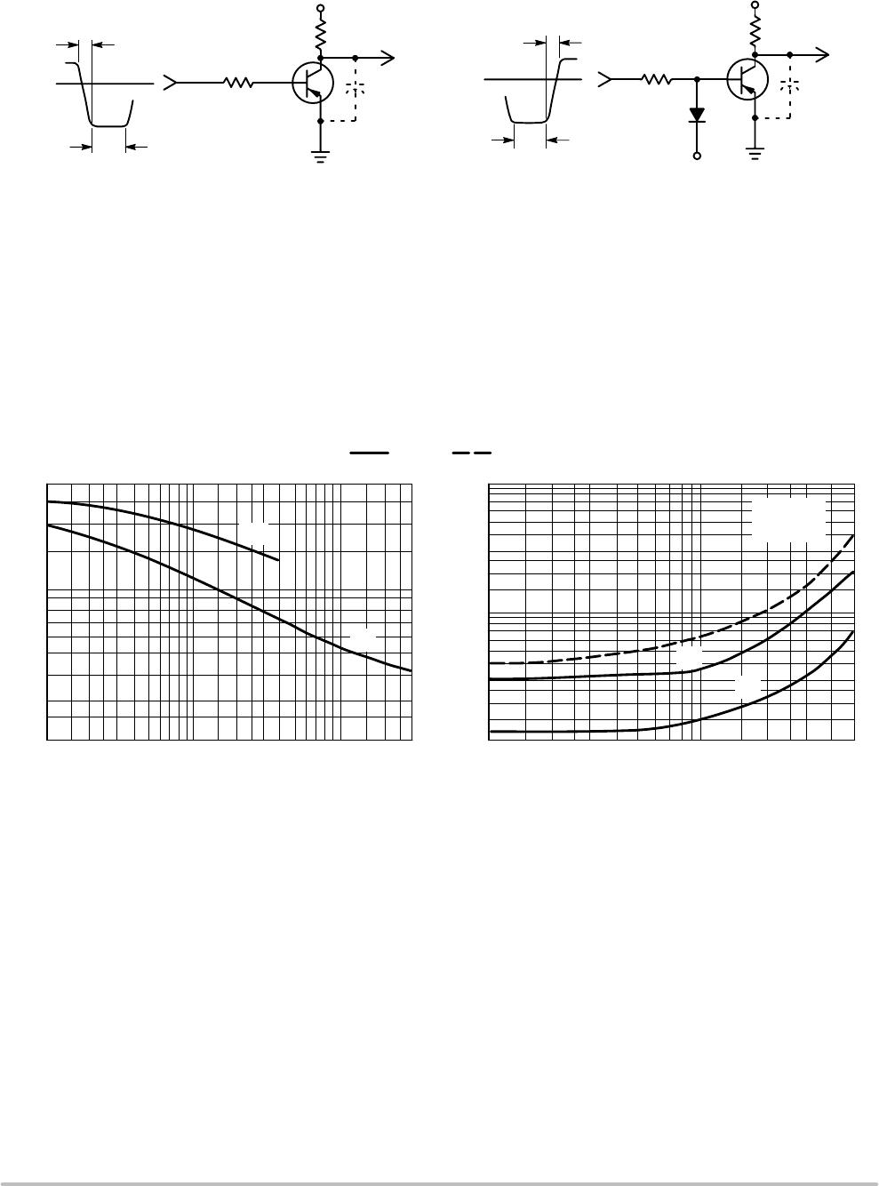
2. Pulse Test: Pulse Width v 300 ms; Duty Cycle v 2.0%.
ON Semiconductort
© Semiconductor Components Industries, LLC, 2006
March, 2006 − Rev. 2
1 Publication Order Number:
MPS3638A/D
MPS3638A
CASE 29−11, STYLE 1
TO−92 (TO−226AA)
1
2
3
COLLECTOR
3
2
BASE
1
EMITTER