NLU3G17BMX1TCG

© Semiconductor Components Industries, LLC, 2016
July, 2016 − Rev. 4
1 Publication Order Number:
NLU3G17/D
NLU3G17
Triple Non-Inverting
Schmitt-Trigger Buffer
The NLU3G17 MiniGatet is an advanced high−speed CMOS
triple non−inverting Schmitt−trigger buffer in ultra−small footprint.
The NLU3G17 input and output structures provide protection when
voltages up to 7.0 V are applied, regardless of the supply voltage.
The NLU3G17 can be used to enhance noise immunity or to square
up slowly changing waveforms.
Features
High Speed: t
PD
= 4.0 ns (Typ) @ V
CC
= 5.0 V
Low Power Dissipation: I
CC
= 1 mA (Max) at T
A
= 25°C
Power Down Protection Provided on inputs
Balanced Propagation Delays
Overvoltage Tolerant (OVT) Input and Output Pins
Ultra−Small Packages
These are Pb−Free Devices
IN A2
OUT Y2
1
OUT Y2
IN A1
GND
OUT Y1
IN A2
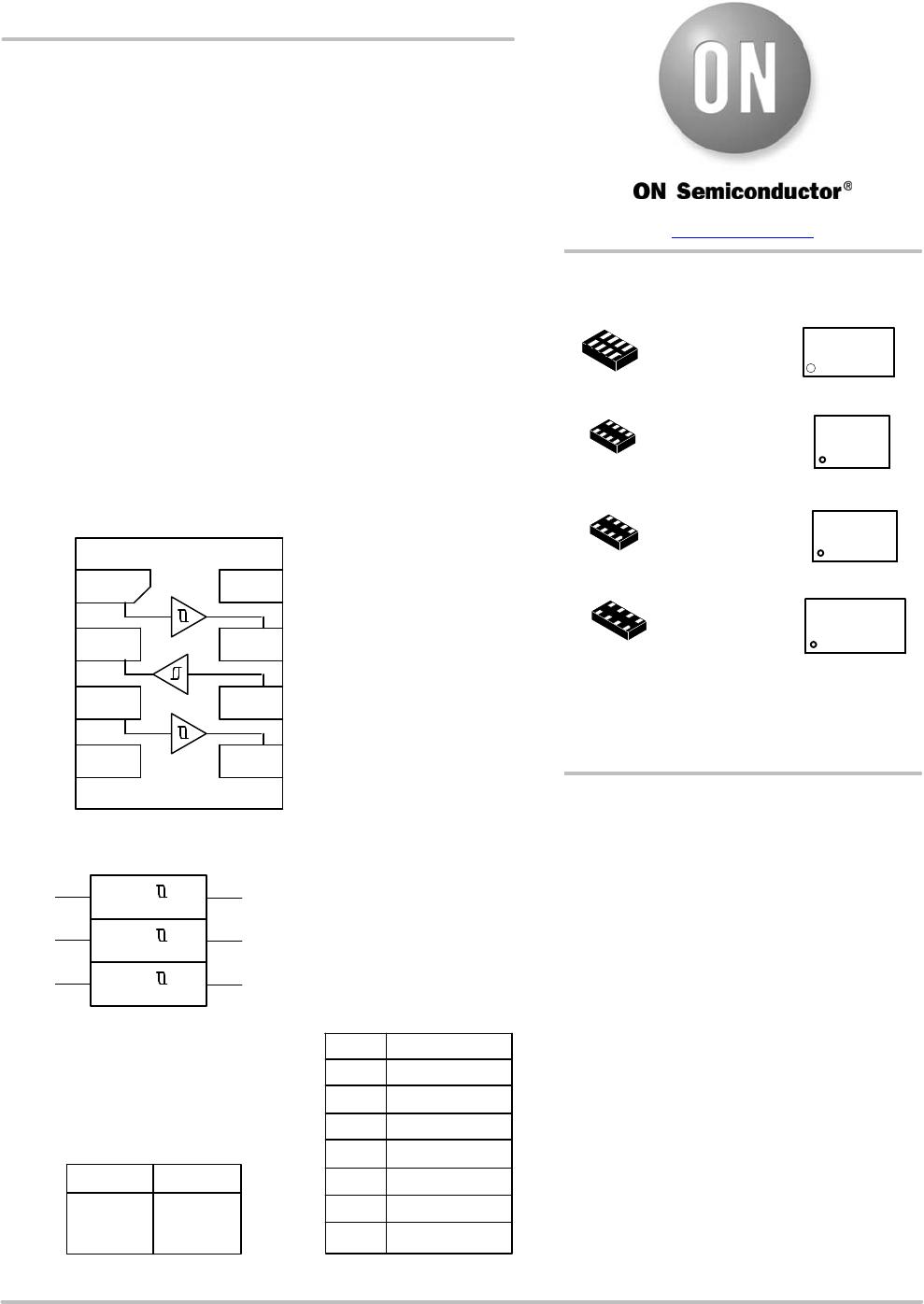
Figure 1. Pinout (Top View)
Figure 2. Logic Symbol
V
CC
IN A1
OUT Y1
1
1
2
3
4
8
7
6
5
OUT Y3
IN A3
IN A3
OUT Y3
1
FUNCTION TABLE
L
H
AY
L
H
PIN ASSIGNMENT
1
2
3IN A2
IN A1
OUT Y3
4
5 OUT Y2
GND
6 IN A3
7 OUT Y1
8V
CC
MARKING
DIAGRAMS
www.onsemi.com
See detailed ordering and shipping information in the package
dimensions section on page 4 of this data sheet.
ORDERING INFORMATION
UDFN8
CASE 517AJ
1
8
UZ, D or LX = Specific Device Code
M = Date Code
G = Pb−Free Package
UZM
G
UDFN8
1.45 x 1.0
CASE 517BZ
UDFN8
1.6 x 1.0
CASE 517BY
UDFN8
1.95 x 1.0
CASE 517CA
X M
1
X M
1
X M
1
NLU3G17
www.onsemi.com
2
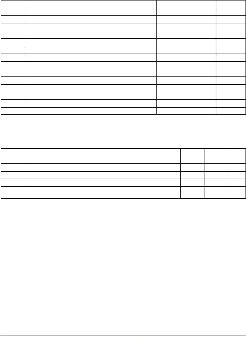
MAXIMUM RATINGS
Symbol Parameter Value Unit
V
CC
DC Supply Voltage −0.5 to +7.0 V
V
IN
DC Input Voltage −0.5 to +7.0 V
V
OUT
DC Output Voltage −0.5 to +7.0 V
I
IK
DC Input Diode Current V
IN
< GND −20 mA
I
OK
DC Output Diode Current V
OUT
< GND ±20 mA
I
O
DC Output Source/Sink Current ±12.5 mA
I
CC
DC Supply Current Per Supply Pin ±25 mA
I
GND
DC Ground Current per Ground Pin ±25 mA
T
STG
Storage Temperature Range −65 to +150 °C
T
L
Lead Temperature, 1 mm from Case for 10 Seconds 260 °C
T
J
Junction Temperature Under Bias 150 °C
MSL Moisture Sensitivity Level 1
F
R
Flammability Rating Oxygen Index: 28 to 34 UL 94 V−0 @ 0.125 in
I
LATCHUP
Latchup Performance Above V
CC
and Below GND at 125°C (Note 2) ±500 mA
Stresses exceeding those listed in the Maximum Ratings table may damage the device. If any of these limits are exceeded, device functionality
should not be assumed, damage may occur and reliability may be affected.
1. Measured with minimum pad spacing on an FR4 board, using 10 mm−by−1 inch, 2 ounce copper trace no air flow.
2. Tested to EIA / JESD78.
RECOMMENDED OPERATING CONDITIONS
Symbol Parameter Min Max Unit
V
CC
Positive DC Supply Voltage 1.65 5.5 V
V
IN
Digital Input Voltage 0 5.5 V
V
OUT
Output Voltage 0 5.5 V
T
A
Operating Free−Air Temperature −55 +125 °C
Dt/DV
Input Transition Rise or Fall Rate V
CC
= 3.3 V ± 0.3 V
V
CC
= 5.0 V ± 0.5 V
0
0
No Limit
No Limit
ns/V
NLU3G17
www.onsemi.com
3
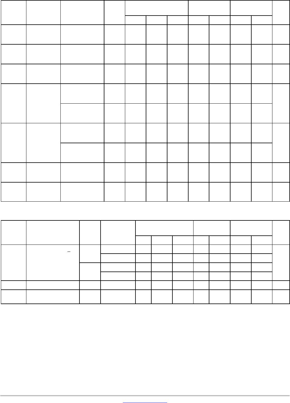
DC ELECTRICAL CHARACTERISTICS
Symbol Parameter Conditions
V
CC
(V)
T
A
= 25 5C T
A
= +855C
T
A
= −555C to
+1255C
Unit
Min Typ Max Min Max Min Max
V
T+
Positive
Threshold
Voltage
3.0
4.5
5.5
1.85
2.86
3.50
2.0
3.0
3.6
2.2
3.15
3.85
2.2
3.15
3.85
2.2
3.15
3.85
V
V
T−
Negative
Threshold
Voltage
3.0
4.5
5.5
0.9
1.35
1.65
1.5
2.3
2.9
1.65
2.46
3.05
0.9
1.35
1.65
0.9
1.35
1.65
V
V
H
Hysteresis
Voltage
3.0
4.5
5.5
0.30
0.40
0.50
0.57
0.67
0.74
1.20
1.40
1.60
0.30
0.40
0.50
1.20
1.40
1.60
0.30
0.40
0.50
1.20
1.40
1.60
V
V
OH
Minimum
High−Level
Output
Voltage
V
IN
w V
T+MAX
I
OH
= −50 mA
2.0
3.0
4.5
1.9
2.9
4.4
2.0
3.0
4.5
1.9
2.9
4.4
1.9
2.9
4.4
V
V
IN
w V
T+MAX
I
OH
= −4 mA
I
OH
= −8 mA
3.0
4.5
2.58
3.94
2.48
3.80
2.34
3.66
V
OL
Maximum
Low−Level
Output
Voltage
V
IN
v V
T−MIN
I
OL
= 50 mA
2.0
3.0
4.5
0
0
0
0.1
0.1
0.1
0.1
0.1
0.1
0.1
0.1
0.1
V
V
IN
v V
T−MIN
I
OL
= 4 mA
I
OL
= 8 mA
3.0
4.5
0.36
0.36
0.44
0.44
0.52
0.52
I
IN
Input
Leakage
Current
0 v V
IN
v 5.5 V 0 to
5.5
±0.1 ±1.0 ±1.0
mA
I
CC
Quiescent
Supply
Current
0 v V
IN
v V
CC
5.5 1.0 10 40
mA
AC ELECTRICAL CHARACTERISTICS (Input t
r
= t
f
= 3.0 ns)
Symbol
Parameter
V
CC
(V)
Test
Condition
T
A
= 25 5C T
A
= +855C
T
A
= −555C to
+1255C
Unit
Min Typ Max Min Max Min Max
t
PLH
,
t
PHL
Propagation Delay,
Input A to Output Y
3.0 to
3.6
C
L
= 15 pF 7.0 12.8 1.0 15 1.0 17
ns
C
L
= 50 pF 8.5 16.3 1.0 18.5 1.0 20.5
4.5 to
5.5
C
L
= 15 pF 4.0 8.6 1.0 10 1.0 11.5
C
L
= 50 pF 5.5 10.6 1.0 12 1.0 13.5
C
IN
Input Capacitance 5.0 10 10 10 pF
C
PD
Power Dissipation
Capacitance (Note 3)
5.0 7.0 pF
3. C
PD
is defined as the value of the internal equivalent capacitance which is calculated from the dynamic operating current consumption without
load. Average operating current can be obtained by the equation I
CC(OPR)
= C
PD
V
CC
f
in
+ I
CC
. C
PD
is used to determine the no−load
dynamic power consumption: P
D
= C
PD
V
CC
2
f
in
+ I
CC
V
CC.

NLU3G17BMX1TCG

Mfr. #:
Manufacturer:
ON Semiconductor
Description:
Buffers & Line Drivers TRPLE NON INVRT SCHM
Lifecycle:
New from this manufacturer.
Delivery:
DHL FedEx Ups TNT EMS
Payment:
T/T Paypal Visa MoneyGram Western Union