MAX9370/MAX9371/MAX9372
LVTTL/TTL-to-Differential LVPECL/PECL
Translators
2 _______________________________________________________________________________________
ABSOLUTE MAXIMUM RATINGS
Stresses beyond those listed under “Absolute Maximum Ratings” may cause permanent damage to the device. These are stress ratings only, and functional
operation of the device at these or any other conditions beyond those indicated in the operational sections of the specifications is not implied. Exposure to
absolute maximum rating conditions for extended periods may affect device reliability.
V
CC
to GND (MAX9370/MAX9371) .......................-0.3V to +5.5V
V
CC
to GND (MAX9372)........................................-0.3V to +4.0V
D_ to GND ..................................................-0.3V to (V
CC
+ 0.3V)
Q_,
Q_ to GND ...........................................-0.3V to (V
CC
+ 0.3V)
Continuous Output Current ................................................50mA
Surge Output Current........................................................100mA
Junction-to-Ambient Thermal Resistance in Still Air
8-Pin SOT23..............................................................+112°C/W
8-Pin µMAX…............................................................+221°C/W
8-Pin SO....................................................................+170°C/W
Junction-to-Ambient Thermal Resistance with
500LFPM Airflow
8-Pin SOT23................................................................+78°C/W
8-Pin µMAX…............................................................+155°C/W
8-Pin SO......................................................................+99°C/W
Junction-to-Case Thermal Resistance
8-Pin SOT23................................................................+80°C/W
8-Pin µMAX…..............................................................+39°C/W
8-Pin SO......................................................................+40°C/W
Continuous Power Dissipation (T
A
= +70°C)
8-Pin SO (derate 5.9mW/°C above +70°C)...................470mW
8-Pin µMAX (derate 4.5mW/°C above +70°C) ..............362mW
8-Pin SOT23 (derate 8.9mW/°C above +70°C).............714mW
Operating Temperature Range ...........................-40°C to +85°C
Junction Temperature .....................................................+150°C
Storage Temperature Range .............................-60°C to +150°C
Soldering Temperature (10s) ...........................................+300°C
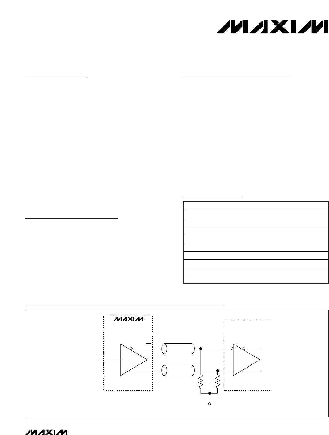
DC ELECTRICAL CHARACTERISTICS
(V
CC
= 3.0V to 5.25V for MAX9370/MAX9371, V
CC
= 3.0V to 3.6V for MAX9372, outputs terminated with 50Ω ±1% to V
CC
- 2.0V.
Typical values are at V
CC
= 3.3V, V
IH
= 2.4V, V
IL
= 0.4V, unless otherwise noted.) (Notes 1, 2, 3)