MAX9372EKA+T

MAX9370/MAX9371/MAX9372
LVTTL/TTL-to-Differential LVPECL/PECL
Translators
4 _______________________________________________________________________________________
Typical Operating Characteristics
(MAX9371, V
CC
= 3.3V, V
IH
= 2.4V, V
IL
= 0.4V, outputs terminated with 50 to V
CC
- 2V, input transition time = 125ps (20% to 80%),
T
A
= +25°C, unless otherwise noted.)
SUPPLY CURRENT vs. TEMPERATURE
MAX9370 toc01
TEMPERATURE (°C)
SUPPLY CURRENT (mA)
603510-15
10
14
18
22
26
6
-40 85
ALL INPUTS AND OUTPUTS ARE OPEN
MAX9370/MAX9372
MAX9371
DIFFERENTIAL OUTPUT VOLTAGE
(V
OH
- V
OL
) vs. FREQUENCY
MAX9370 toc02
FREQUENCY (GHz)
DIFFERENTIAL OUTPUT VOLTAGE (mV)
1.61.20.80.4
200
400
600
800
1000
0
02.0
TRANSITION TIME vs. TEMPERATURE
MAX9370 toc03
TEMPERATURE (°C)
TRANSITION TIME (ps)
603510-15
200
220
240
260
180
-40 85
f = 100MHz
FALLING EDGE
RISING EDGE
PROPAGATION DELAY vs. TEMPERATURE
MAX9370 toc04
TEMPERATURE (°C)
PROPAGATION DELAY (ps)
603510-15
250
260
270
280
290
300
240
-40 85
Detailed Description
The MAX9370/MAX9371/MAX9372 LVTTL/TTL-to-differ-
ential LVPECL/PECL translators are designed for high-
speed communication signal and clock driver
applications. The MAX9370/MAX9372 are dual LVTTL-
to-LVPECL/PECL translators that operate in excess of
1GHz. The MAX9371 is a single translator. The
MAX9370/MAX9371 operate over a wide 3.0V to 5.25V
supply range, allowing high-performance clock or data
distribution in systems with a nominal 3.3V or 5.0V sup-
ply. The MAX9372 is optimized for 3.0V to 3.6V opera-
tion. These devices feature low 270ps propagation
delay and 40ps peak-to-peak deterministic jitter.
Inputs and Outputs
The MAX9370/MAX9371/MAX9372 inputs accept stan-
dard LVTTL/TTL levels. The input has pullup circuitry that
drives the outputs to a differential high if the inputs are
open. The outputs are differential LVPECL/PECL levels.
Applications Information
Output Termination
Terminate outputs with 50 to V
CC
- 2V or use an equiv-
alent Thevenin termination. Use the same terminate on
each output for the lowest output-to-output skew. When a
single-ended signal is taken from a differential output,
terminate both outputs. For example, if Q is used as a
single-ended output, terminate both Q and Q.
MAX9370/MAX9371/MAX9372
LVTTL/TTL-to-Differential LVPECL/PECL
Translators
_______________________________________________________________________________________ 5
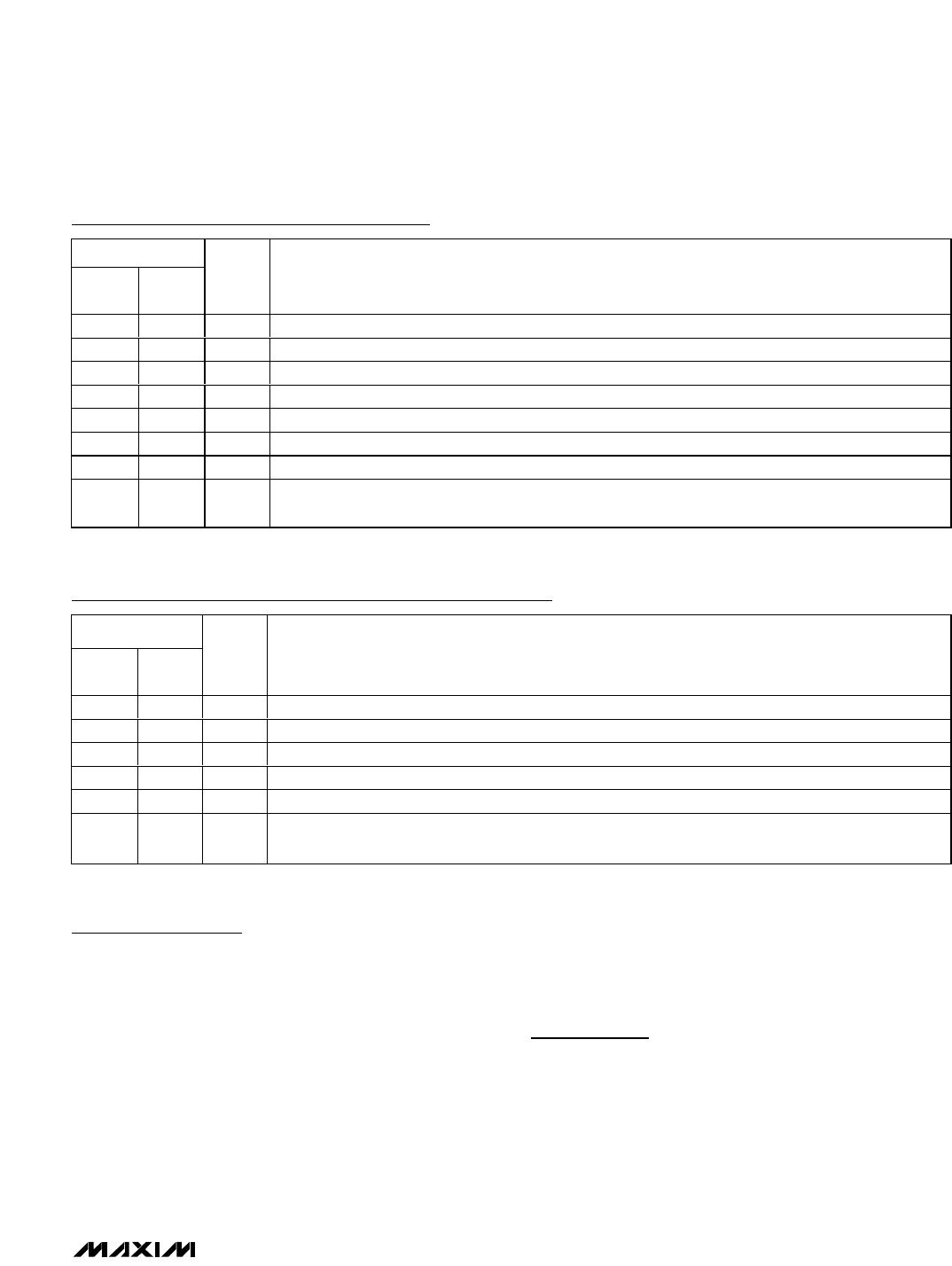
Pin Description for the MAX9370/MAX9372
PIN
SO
µMAX
SOT23
NAME
FUNCTION
1 8 Q0 Noninverting Differential LVPECL/PECL Output 0. Typically terminate with 50 resistor to V
CC
- 2V.
27Q0 Inverting Differential LVPECL/PECL Output 0. Typically terminate with 50 resistor to V
CC
- 2V.
3 6 Q1 Noninverting Differential LVPECL/PECL Output 1. Typically terminate with 50 resistor to V
CC
- 2V.
45Q1 Inverting Differential LVPECL/PECL Output 1. Typically terminate with 50 resistor to V
CC
- 2V.
52
GND
Ground. Provide a low-impedance connection to ground plane.
6 4 D1 LVTTL/TTL Input 1. LVTTL/TTL input for translator corresponding to output Q1 and Q1.
7 3 D0 LVTTL/TTL Input 0. LVTTL/TTL input for translator corresponding to output Q0 and Q0.
81V
CC
Positive Supply Voltage. Bypass V
CC
to GND with 0.1µF and 0.01µF ceramic capacitors. Place the
capacitors as close to the device as possible with the smaller value capacitor closest to the device.
Pin Description for the MAX9371
PIN
SO
µMAX
SOT23
NAME
FUNCTION
1, 4, 6
4, 5, 8 N.C.
No Connection. No internal connection.
2 7 Q Noninverting Differential LVPECL/PECL Output. Typically terminate with 50 resistor to V
CC
- 2V.
36Q Inverting Differential LVPECL/PECL Output. Typically terminate with 50 resistor to V
CC
- 2V.
52
GND
Ground. Provide a low-impedance connection to ground plane.
7 3 D LVTTL/TTL Input
81
V
CC
Positive Supply Voltage. Bypass V
CC
to GND with 0.1µF and 0.01µF ceramic capacitors. Place the
capacitors as close to the device as possible with the smaller value capacitor closest to the device.
MAX9370/MAX9371/MAX9372
Ensure that the output currents do not exceed the con-
tinuous safe output current limit or surge output current
limit as specified in the Absolute Maximum Ratings
table. Under all operating conditions, the devices total
thermal limits should be observed.
Supply Bypassing
Bypass V
CC
to GND with high-frequency surface-mount
ceramic 0.1µF and 0.01µF capacitors in parallel and as
close to the device as possible, with the 0.01µF capaci-
tor closest to the device. Use multiple parallel vias to
minimize parasitic inductance.
PC Board Traces
Input and output trace characteristics affect the perfor-
mance of the MAX9370/MAX9371/MAX9372. Connect
each differential output to a 50 characteristic impedance
trace. Minimize the number of vias to prevent impedance
discontinuities. Reduce reflections by maintaining the 50
characteristic impedance through connectors and across
cables. Reduce skew within a differential pair by match-
ing the electrical length of the traces.
Chip Information
TRANSISTOR COUNT: 358
PROCESS: Bipolar
LVTTL/TTL-to-Differential LVPECL/PECL
Translators
6 _______________________________________________________________________________________
D_
0V (DIFFERENTIAL)
20%
80%
20%
80%
t
R
t
F
Q_
Q_
Q_ - Q_
V
IH
V
IL
50%
t
PLH
50%
V
OH
V
OL
V
OH
- V
OL
V
OH
- V
OL
V
OH
- V
OL
t
PHL
Figure 1. Input-to-Output Propagation Delay and Transition Timing Diagram

MAX9372EKA+T

Mfr. #:
Manufacturer:
Maxim Integrated
Description:
Translation - Voltage Levels LVTTL/TTL-to-Diff LVPECL/PECL Trans
Lifecycle:
New from this manufacturer.
Delivery:
DHL FedEx Ups TNT EMS
Payment:
T/T Paypal Visa MoneyGram Western Union