TLP705A
4
9.
9.
9.
9. Electrical Characteristics (Note)
Electrical Characteristics (Note)
Electrical Characteristics (Note)
Electrical Characteristics (Note)
(Unless otherwise specified, T
(Unless otherwise specified, T
(Unless otherwise specified, T
(Unless otherwise specified, T
a
a
a
a
= -40 to 100
= -40 to 100
= -40 to 100
= -40 to 100
)
)
)
)
Characteristics
Input forward voltage
Input forward voltage
temperature coefficient
Input reverse current
Input capacitance
Peak high-level output current
Peak low-level output current
High-level output voltage
Low-level output voltage
High-level supply current
Low-level supply current
Threshold input current (L/H)
Threshold input voltage (H/L)
Supply voltage
Symbol
V
F
∆V
F
/∆T
a
I
R
C
t
I
OPH
I
OPL
V
OH
V
OL
I
CCH
I
CCL
I
FLH
V
FHL
V
CC
Note
(Note 1)
(Note 1)
Test
Circuit
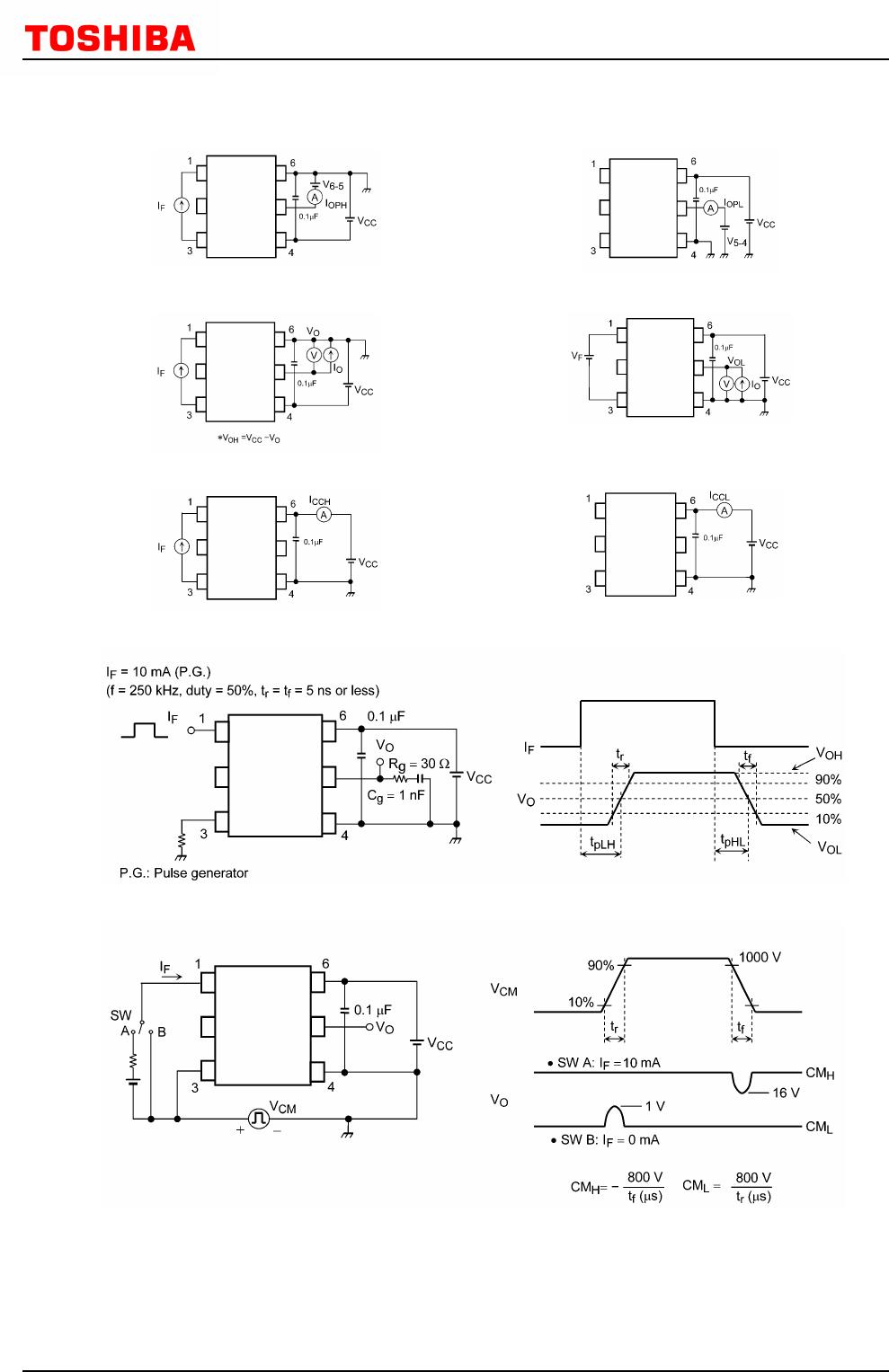
Fig.
12.1.1
Fig.
12.1.2
Fig.
12.1.3
Fig.
12.1.4
Fig.
12.1.5
Fig.
12.1.6
Test Condition
I
F
= 10 mA, T
a
= 25
I
F
= 10 mA
V
R
= 5 V, T
a
= 25
V = 0 V, f = 1 MHz, T
a
= 25
I
F
= 10 mA, V
CC
= 15 V,
V
6-5
= 4 V
I
F
= 10 mA, V
CC
= 15 V,
V
6-5
= 10 V
I
F
= 0 mA, V
CC
= 15 V,
V
5-4
= 2 V
I
F
= 0 mA, V
CC
= 15 V,
V
5-4
= 10 V
I
F
= 10 mA, V
CC
= 10 V,
I
O
= -100 mA
V
F
= 0.8 V, V
CC
= 10 V,
I
O
= 100 mA
I
F
= 10 mA, V
CC
= 10 to 30 V,
V
O
= Open
I
F
= 0 mA, V
CC
= 10 to 30 V,
V
O
= Open
V
CC
= 15 V, V
O
> 1 V
V
CC
= 15 V, V
O
< 1 V
Min
1.40
0.2
0.4
6.0
0.8
10
Typ.
1.57
-1.8
60
-0.32
-0.6
0.32
0.6
8.5
0.35
Max
1.80
10
-0.2
-0.4
1.0
3.0
3.0
7.5
30
Unit
V
mV/
µA
pF
A
V
mA
V
Note: All typical values are at T
a
= 25 .
Note: This device is designed for low power consumption, making it more sensitive to ESD than its predecessors.
Extra care should be taken in the design of circuitry and pc board implementation to avoid ESD problems.
Note 1: I
O
application time ≤ 50 µs, single pulse.
10.
10.
10.
10. Isolation Characteristics (Unless otherwise specified, T
Isolation Characteristics (Unless otherwise specified, T
Isolation Characteristics (Unless otherwise specified, T
Isolation Characteristics (Unless otherwise specified, T
a
a
a
a
= 25
= 25
= 25
= 25
)
)
)
)
Characteristics
Total capacitance (input to output)
Isolation resistance
Isolation voltage
Symbol
C
S
R
S
BV
S
Note
(Note 1)
(Note 1)
(Note 1)
Test Conditions
V
S
= 0 V, f = 1 MHz
V
S
= 500 V, R.H. ≤ 60 %
AC, 60 s
AC, 1 s in oil
DC, 60 s in oil
Min
1 × 10
12
5000
Typ.
1.0
10
14
10000
10000
Max
Unit
pF
Ω
Vrms
Vdc
Note 1: This device is considered as a two-terminal device: Pins 1, 2 and 3 are shorted together, and pins 4, 5 and 6
are shorted together.
2015-12-25
Rev.5.0
©2015 Toshiba Corporation