TC74VCX157FT/FK
2014-03-01 1
TOSHIBA CMOS Digital Integrated Circuit Silicon Monolithic
TC74VCX157FT, TC74VCX157FK
Low Voltage Quad 2-Channel Multiplexer with 3.6 V Tolerant Inputs and Outputs
The TC74VCX157 is a high performance CMOS multiplexer
which is guaranteed to operate from 1.2-V to 3.6-V. Designed for
use in 1.5 V, 1.8 V, 2.5 V or 3.3 V systems, it achieves high. speed
operation while maintaining the CMOS low power dissipation.
It is also designed with over voltage tolerant inputs and outputs
up to 3.6 V.
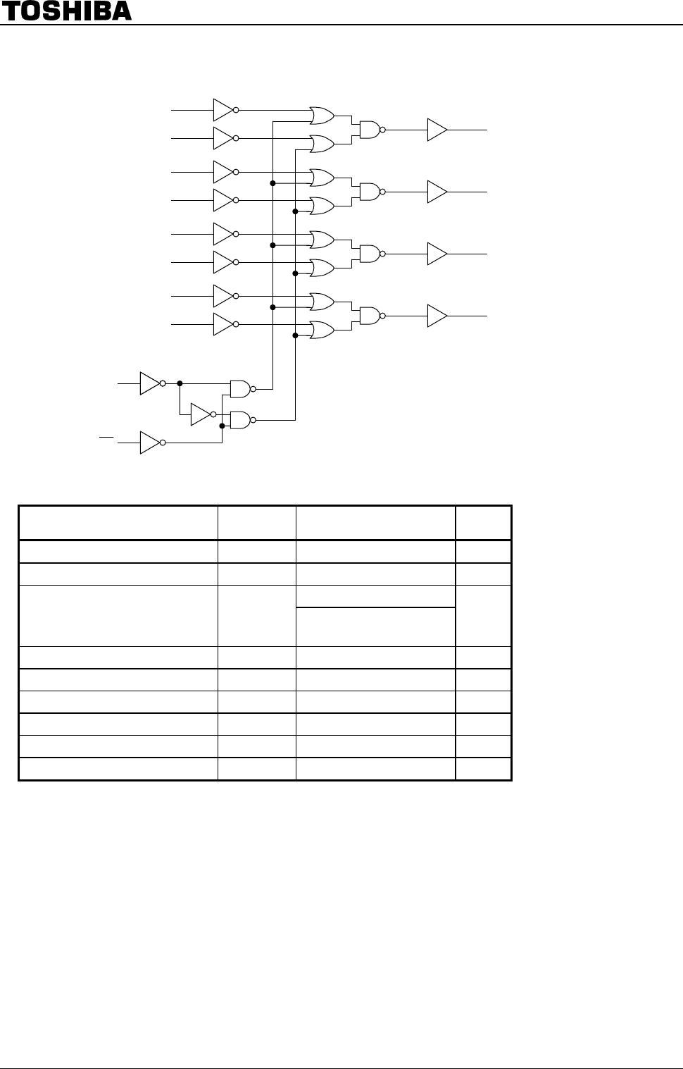
It consists of four 2-input digital multiplexers with common
select and strobe inputs.
When the ST input is held “H” level, selection of data is
inhibited and all the outputs become “L” level. The SELECT
decoding determines whether the A or B inputs get routed to their
corresponding Y outputs.
All inputs are equipped with protection circuits against static
discharge.
Features
• Low voltage operation: V
CC
= 1.2 to 3.6 V
• High speed operation: t
pd
= 3.0 ns (max) (V
CC
= 3.0 to 3.6 V)
t
pd
= 3.5 ns (max) (V
CC
= 2.3 to 2.7 V)
t
pd
= 7.0 ns (max) (V
CC
= 1.65 to 1.95 V)
t
pd
= 14.0 ns (max) (V
CC
= 1.4 to 1.6 V)
t
pd
= 35.0 ns (max) (V
CC
= 1.2 V)
• 3.6 V tolerant inputs and outputs.
• Output current: I
OH
/I
OL
= ±24 mA (min) (V
CC
= 3.0 V)
I
OH
/I
OL
= ±18 mA (min) (V
CC
= 2.3 V)
I
OH
/I
OL
= ±6 mA (min) (V
CC
= 1.65 V)
I
OH
/I
OL
= ±2 mA (min) (V
CC
= 1.4 V)
• Latch-up performance: −300 mA
• ESD performance: Machine model ≥ ±200 V
Human body model ≥ ±2000 V
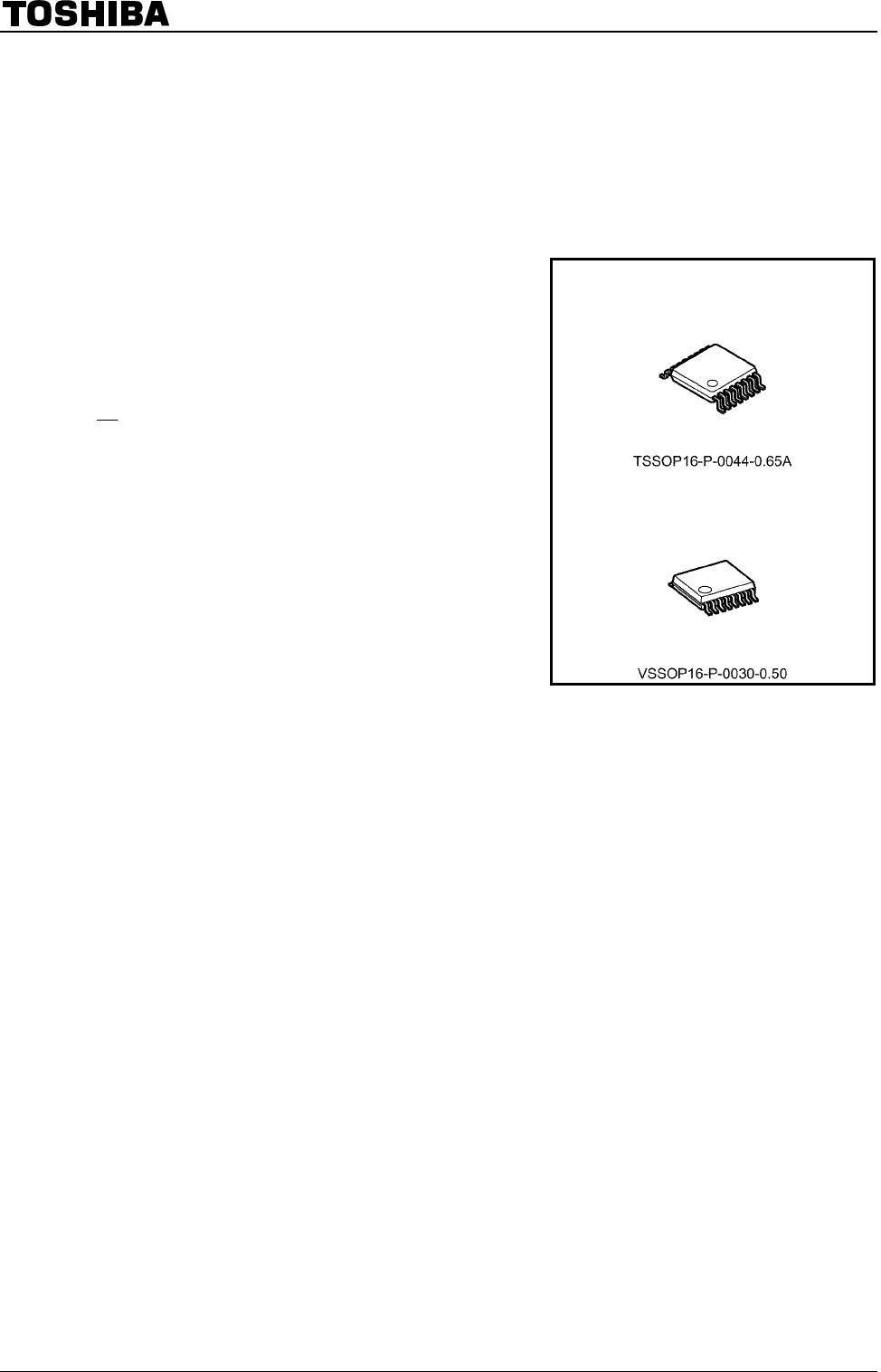
• Package: TSSOP and VSSOP (US)
• Power down protection is provided on all inputs and outputs.
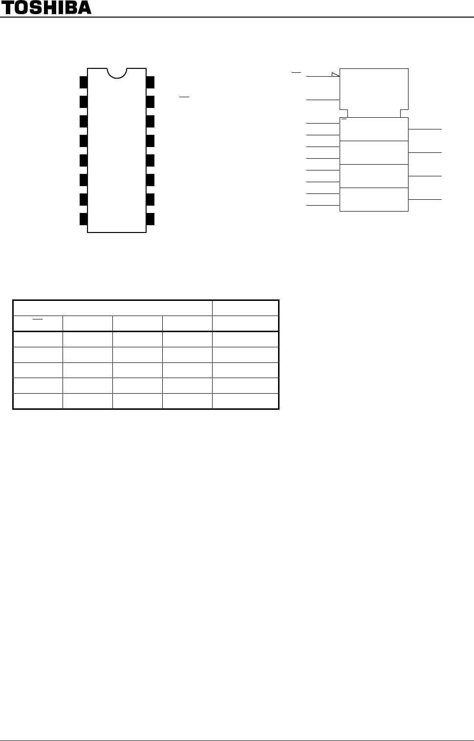
TC74VCX157FT
TC74VCX157FK
Weight
TSSOP16-P-0044-0.65A : 0.06 g (typ.)
VSSOP16-P-0030-0.50 : 0.02 g (typ.)
Start of commercial production
1999-07