5/7/03
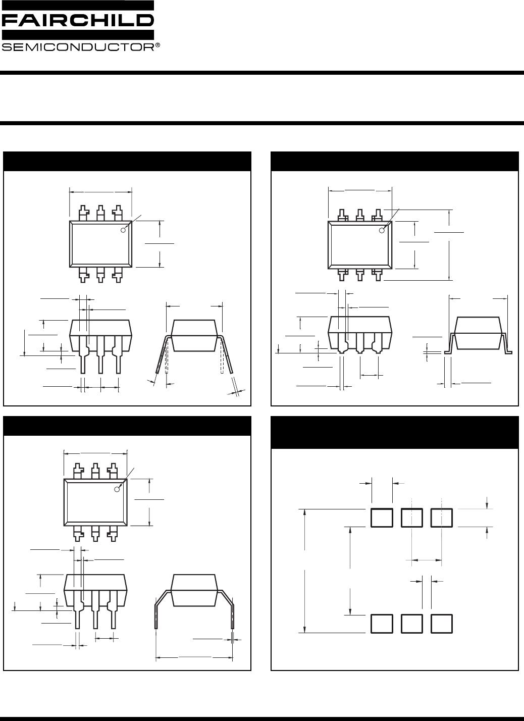
4N25 4N26 4N27 4N28 4N35 4N36
4N37 H11A1 H11A2 H11A3 H11A4 H11A5
GENERAL PURPOSE 6-PIN
PHOTOTRANSISTOR OPTOCOUPLERS
Page 12 of 15
© 2003 Fairchild Semiconductor Corporation
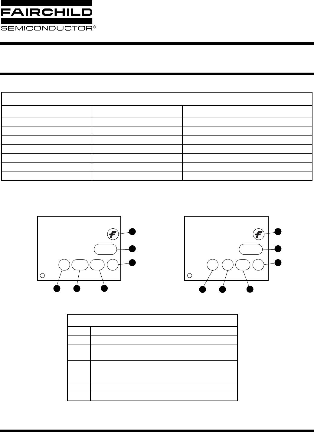
ORDERING INFORMATION
MARKING INFORMATION
Order Entry Identifier
Black Package (No Suffix) White Package (-M Suffix) Option
.S S Surface Mount Lead Bend
.SD SR2 Surface Mount; Tape and reel
.W T 0.4" Lead Spacing
.300 V VDE 0884
.300W TV VDE 0884, 0.4" Lead Spacing
.3S SV VDE 0884, Surface Mount
.3SD SR2V VDE 0884, Surface Mount, Tape & Reel
4N25
V XX YY K
Black Package, No Suffix
1
2
6
43
5
4N25
V X YY Q
White Package, -M Suffix
1
2
6
43
5
*Note – Parts built in the white package (M suffix) that do not have the ‘V’ option (see
definition 3 above) that are marked with date code ‘325’ or earlier are marked in the
portrait format.
Definitions
1 Fairchild logo
2 Device number
3
VDE mark (Note: Only appears on parts ordered with VDE
option – See order entry table)
4
One or two digit year code
• Two digits for black package parts, e.g., ‘03’
• One digit for white package parts, e.g., ‘3’
5 Two digit work week ranging from ‘01’ to ‘53’
6 Assembly package code