General Description
The DS1990A serial number iButton
®
is a rugged data
carrier that serves as an electronic registration number
for automatic identification. Data is transferred serially
through the 1-Wire
®
protocol, which requires only a sin-
gle data lead and a ground return. Every DS1990A is
factory lasered with a guaranteed unique 64-bit regis-
tration number that allows for absolute traceability. The
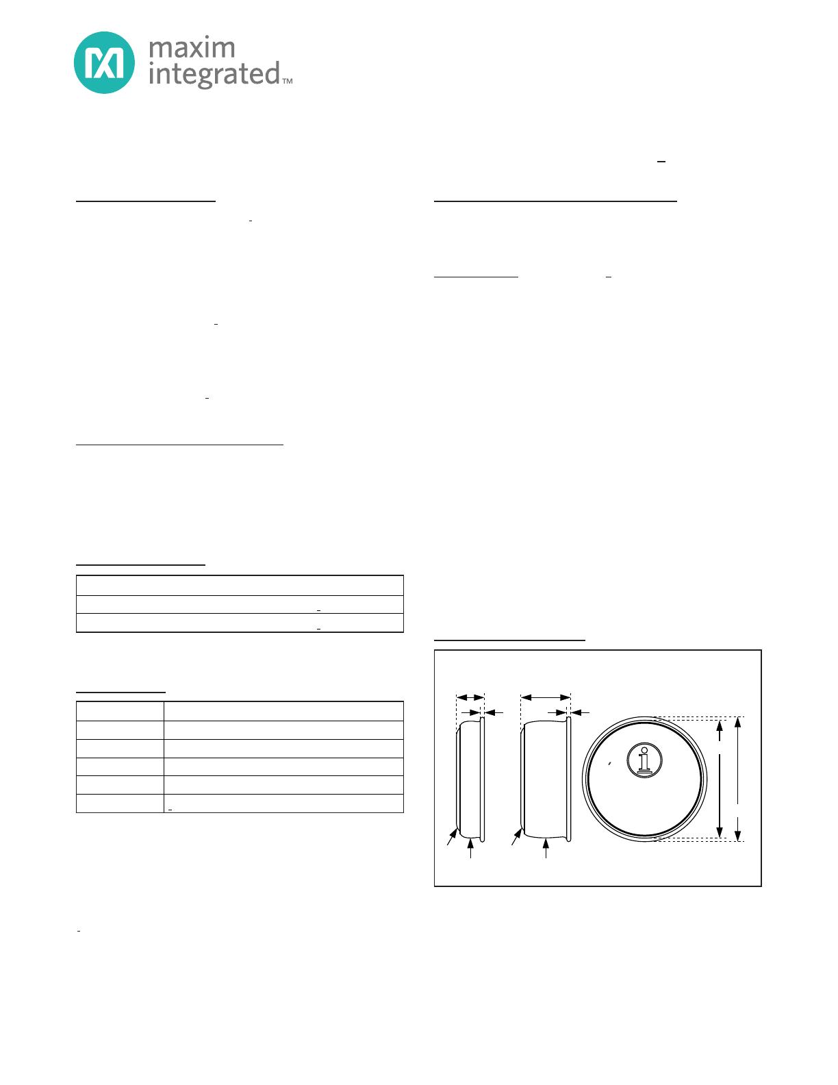
durable stainless-steel iButton package is highly resis-
tant to environmental hazards such as dirt, moisture,
and shock. Its compact coin-shaped profile is self-
aligning with mating receptacles, allowing the DS1990A
to be used easily by human operators. Accessories
enable the DS1990A iButton to be mounted on almost
any object, including containers, pallets, and bags.
Applications
Access Control
Work-In-Progress Tracking
Tool Management
Inventory Control
Features
♦ Can Be Read in Less Than 5ms
♦ Operating Range: 2.8V to 6.0V, -40°C to +85°C
Common iButton Features
♦ Unique Factory-Lasered 64-Bit Registration
Number Ensures Error-Free Device Selection and
Absolute Traceability Because No Two Parts are
Alike
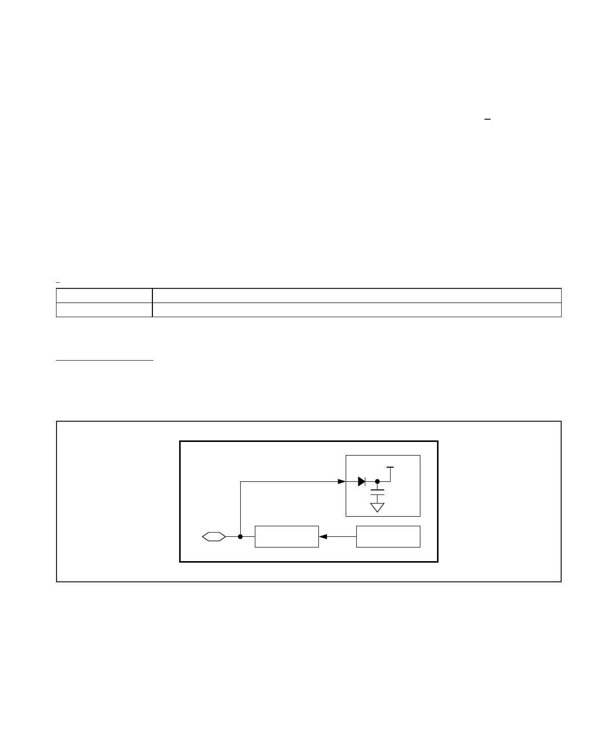
♦ Built-In Multidrop Controller for 1-Wire Net
♦ Digital Identification by Momentary Contact
♦ Data Can Be Accessed While Affixed to Object
♦ Economically Communicates to Bus Master with
a Single Digital Signal at 16.3kbps
♦ Button Shape is Self-Aligning with Cup-Shaped
Probes
♦ Durable Stainless-Steel Case Engraved with
Registration Number Withstands Harsh
Environments
♦ Easily Affixed with Self-Stick Adhesive Backing,
Latched by its Flange, or Locked with a Ring
Pressed Onto its Rim
Serial Number i
Button
Pin Configurations