1
LT1352/LT1353
13523fa
TYPICAL APPLICATIO
U
APPLICATIO S
U
DESCRIPTIO
U
FEATURES
Dual and Quad
250µA, 3MHz, 200V/µs
Operational Amplifiers
3MHz Gain Bandwidth
200V/µs Slew Rate
250µA Supply Current per Amplifier
C-Load
TM
Op Amp Drives All Capacitive Loads
Unity-Gain Stable
Maximum Input Offset Voltage: 600µV
Maximum Input Bias Current: 50nA
Maximum Input Offset Current: 15nA
Minimum DC Gain, R
L
= 2k: 30V/mV
Input Noise Voltage: 14nV/Hz
Settling Time to 0.1%, 10V Step: 700ns
Settling Time to 0.01%, 10V Step: 1.25µs
Minimum Output Swing into 1k: ±13V
Minimum Output Swing into 500: ±3.4V
Specified at ±2.5V, ±5V and ±15V
Battery-Powered Systems
Wideband Amplifiers
Buffers
Active Filters
Data Acquisition Systems
Photodiode Amplifiers
The LT
®
1352/LT1353 are dual and quad, very low power,
high speed operational amplifiers with outstanding AC
and DC performance. The amplifiers feature much lower
supply current and higher slew rate than devices with
comparable bandwidth. The circuit combines the slewing
performance of a current feedback amplifier in a true
operational amplifier with matched high impedance
inputs. The high slew rate ensures that the large-signal
bandwidth is not degraded. Each output is capable of
driving a 1k load to ±13V with ±15V supplies and a 500
load to ±3.4V on ±5V supplies.
The LT1352/LT1353 are members of a family of fast, high
performance amplifiers using this unique topology and
employing Linear Technology Corporation’s advanced
complementary bipolar processing. For higher bandwidth
devices with higher supply current see the LT1354 through
LT1365 data sheets. Bandwidths of 12MHz, 25MHz, 50MHz
and 70MHz are available with 1mA, 2mA, 4mA and 6mA of
supply current per amplifier. Singles, duals and quads of
each amplifier are available. The LT1352 is available in an
8-lead SO package. The LT1353 is offered in a 14-lead
narrow surface mount package.
C-Load is a trademark of Linear Technology Corporation.
, LTC and LT are registered trademarks of Linear Technology Corporation.
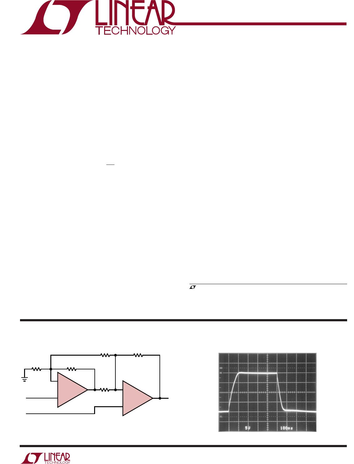
Instrumentation Amplifier
Large-Signal Response
A
V
= –1 1352/53 TA02
+
GAIN = [R4/R3][1 + (1/2)(R2/R1 + R3/R4) + (R2 + R3)/R5] = 102
TRIM R5 FOR GAIN
TRIM R1 FOR COMMON MODE REJECTION
BW = 30kHz
+
1/2
LT1352
+
1/2
LT1352
R1
50k
R2
5k
R5
1.1k
R3
5k
R4
50k
V
IN
V
OUT
1352/53 TA01
Available in SO-8 Package
LT1353 in Narrow Surface Mount Package
2
LT1352/LT1353
13523fa
Consult LTC Marketing for parts specified with wider operating temperature ranges.
SYMBOL PARAMETER CONDITIONS V
SUPPLY
MIN TYP MAX UNITS
V
OS
Input Offset Voltage ±15V 0.2 0.6 mV
±5V 0.2 0.6 mV
±2.5V 0.3 0.8 mV
I
OS
Input Offset Current ±2.5V to ±15V 5 15 nA
I
B
Input Bias Current ±2.5V to ±15V 20 50 nA
e
n
Input Noise Voltage f = 10kHz ±2.5V to ±15V 14 nV/Hz
i
n
Input Noise Current f = 10kHz ±2.5V to ±15V 0.5 pA/Hz
R
IN
Input Resistance V
CM
= ±12V ±15V 300 600 M
Differential ±15V 20 M
C
IN
Input Capacitance ±15V 3 pF
Positive Input Voltage Range ±15V 12.0 13.5 V
±5V 2.5 3.5 V
±2.5V 0.5 1.0 V
Negative Input Voltage Range ±15V 13.5 12.0 V
±5V 3.5 2.5 V
±2.5V 1.0 0.5 V
CMRR Common Mode Rejection Ratio V
CM
= ±12V ±15V 80 94 dB
V
CM
= ±2.5V ±5V 78 86 dB
V
CM
= ±0.5V ±2.5V 68 77 dB
PSRR Power Supply Rejection Ratio V
S
= ±2.5V to ±15V 90 106 dB
ABSOLUTE MAXIMUM RATINGS
W
WW
U
Total Supply Voltage (V
+
to V
) .............................. 36V
Differential Input Voltage (Transient Only, Note 2) ±10V
Input Voltage .......................................................... ±V
S
Output Short-Circuit Duration (Note 3)........... Indefinite
Operating Temperature Range ................ 40°C to 85°C
Specified Temperature Range (Note 7).. 40°C to 85°C
Maximum Junction Temperature (See Below)
Plastic Package ............................................... 150°C
Storage Temperature Range ................. 65°C to 150°C
Lead Temperature (Soldering, 10 sec).................. 300°C
ELECTRICAL CHARACTERISTICS
T
A
= 25°C, V
CM
= 0V unless otherwise noted
PACKAGE/ORDER INFORMATION
W
UU
ORDER PART
NUMBER
ORDER PART
NUMBER
LT1352CN8
LT1352CS8
LT1352IN8
LT1352IS8
LT1353CS
TOP VIEW
S PACKAGE
14-LEAD PLASTIC SO
1
2
3
4
5
6
7
14
13
12
11
10
9
8
OUT A
IN A
+IN A
V
+
+IN B
IN B
OUT B
OUT D
IN D
+IN D
V
+IN C
IN C
OUT C
C
B
D
A
T
JMAX
= 150°C, θ
JA
= 150°C/ W
S8 PART MARKING
1352
1352I
1
2
3
4
8
7
6
5
TOP VIEW
OUT A
IN A
+IN A
V
V
+
OUT B
IN B
+IN B
N8 PACKAGE
8-LEAD PDIP
S8 PACKAGE
8-LEAD PLASTIC SO
B
A
T
JMAX
= 150°C, θ
JA
= 130°C/ W (N8)
T
JMAX
= 150°C, θ
JA
= 190°C/ W (S8)
(Note 1)
3
LT1352/LT1353
13523fa
SYMBOL PARAMETER CONDITIONS V
SUPPLY
MIN TYP MAX UNITS
A
VOL
Large-Signal Voltage Gain V
OUT
= ±12V, R
L
= 5k ±15V 40 80 V/mV
V
OUT
= ±10V, R
L
= 2k ±15V 30 60 V/mV
V
OUT
= ±10V, R
L
= 1k ±15V 20 40 V/mV
V
OUT
= ±2.5V, R
L
= 5k ±5V 30 60 V/mV
V
OUT
= ±2.5V, R
L
= 2k ±5V 25 50 V/mV
V
OUT
= ±2.5V, R
L
= 1k ±5V 15 30 V/mV
V
OUT
= ±1V, R
L
= 5k ±2.5V 20 40 V/mV
V
OUT
Output Swing R
L
= 5k, V
IN
= ±10mV ±15V 13.5 14.0 ±V
R
L
= 2k, V
IN
= ±10mV ±15V 13.4 13.8 ±V
R
L
= 1k, V
IN
= ±10mV ±15V 13.0 13.4 ±V
R
L
= 1k, V
IN
= ±10mV ±5V 3.5 4.0 ±V
R
L
= 500, V
IN
= ±10mV ±5V 3.4 3.8 ±V
R
L
= 5k, V
IN
= ±10mV ±2.5V 1.3 1.7 ±V
I
OUT
Output Current V
OUT
= ±13V ±15V 13.0 13.4 mA
V
OUT
= ±3.4V ±5V 6.8 7.6 mA
I
SC
Short-Circuit Current V
OUT
= 0V, V
IN
= ±3V ±15V 30 45 mA
SR Slew Rate A
V
= –1, R
L
= 5k (Note 4) ±15V 120 200 V/µs
±5V 30 50 V/µs
Full-Power Bandwidth 10V Peak (Note 5) ±15V 3.2 MHz
3V Peak (Note 5) ±5V 2.6 MHz
GBW Gain Bandwidth f = 200kHz, R
L
= 10k ±15V 2.0 3.0 MHz
±5V 1.8 2.7 MHz
±2.5V 2.5 MHz
t
r
, t
f
Rise Time, Fall Time A
V
= 1, 10% to 90%, 0.1V ±15V 46 ns
±5V 53 ns
Overshoot A
V
= 1, 0.1V ±15V 13 %
±5V 16 %
Propagation Delay 50% V
IN
to 50% V
OUT
, 0.1V ±15V 41 ns
±5V 52 ns
t
s
Settling Time 10V Step, 0.1%, A
V
= –1 ±15V 700 ns
10V Step, 0.01%, A
V
= –1 ±15V 1250 ns
5V Step, 0.1%, A
V
= –1 ±5V 950 ns
5V Step, 0.01%, A
V
= –1 ±5V 1400 ns
R
O
Output Resistance A
V
= 1, f = 20kHz ±15V 1.5
Channel Separation V
OUT
= ±10V, R
L
= 2k ±15V 101 120 dB
I
S
Supply Current Each Amplifier ±15V 250 320 µA
Each Amplifier ±5V 230 300 µA
ELECTRICAL CHARACTERISTICS
T
A
= 25°C, V
CM
= 0V unless otherwise noted
SYMBOL PARAMETER CONDITIONS V
SUPPLY
MIN TYP MAX UNITS
V
OS
Input Offset Voltage ±15V 0.8 mV
±5V 0.8 mV
±2.5V 1.0 mV
Input V
OS
Drift (Note 6) ±2.5V to ±15V 3 8 µV/°C
I
OS
Input Offset Current ±2.5V to ±15V 20 nA
I
B
Input Bias Current ±2.5V to ±15V 75 nA
0°C T
A
70°C, V
CM
= 0V unless otherwise noted

LT1352IS8#TRPBF

Mfr. #:
Manufacturer:
Analog Devices Inc.
Description:
Operational Amplifiers - Op Amps Dual 250uA 3MHz 200V/us OA
Lifecycle:
New from this manufacturer.
Delivery:
DHL FedEx Ups TNT EMS
Payment:
T/T Paypal Visa MoneyGram Western Union