10
LT1352/LT1353
13523fa
APPLICATIONS INFORMATION
WUU
U
applications where DC accuracy must be maximized. The
inputs can withstand transient differential input voltages
up to 10V without damage and need no clamping or source
resistance for protection. Differential inputs, however,
generate large supply currents (tens of mA) as required for
high slew rates. If the device is used with sustained
differential inputs, the average supply current will in-
crease, excessive power dissipation will result and the part
may be damaged. The part should not be used as a
comparator, peak detector or other open-loop applica-
tion with large, sustained differential inputs. Under
normal, closed-loop operation, an increase of power dis-
sipation is only noticeable in applications with large slewing
outputs and is proportional to the magnitude of the
differential input voltage and the percent of time that the
inputs are apart. Measure the average supply current for
the application in order to calculate the power dissipation.
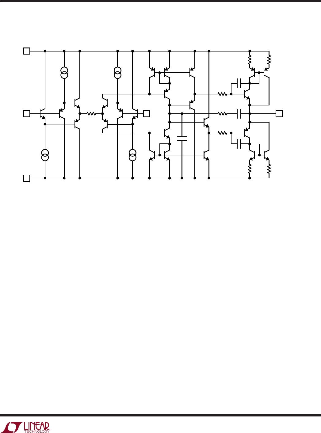
Circuit Operation
The LT1352/LT1353 circuit topology is a true voltage
feedback amplifier that has the slewing behavior of a
current feedback amplifier. The operation of the circuit can
be understood by referring to the Simplified Schematic.
The inputs are buffered by complementary NPN and PNP
emitter followers which drive R1, a 1k resistor. The input
voltage appears across the resistor generating currents
which are mirrored into the high impedance node and
compensation capacitor C
T
. Complementary followers
form an output stage which buffers the gain node from the
load. The output devices Q19 and Q22 are connected to
form a composite PNP and a composite NPN.
The bandwidth is set by the input resistor and the capaci-
tance on the high impedance node. The slew rate is
determined by the current available to charge the high
impedance node capacitance. This current is the differen-
tial input voltage divided by R1, so the slew rate is
proportional to the input. Highest slew rates are therefore
seen in the lowest gain configurations. For example, a 10V
output step in a gain of 10 has only a 1V input step whereas
the same output step in unity gain has a 10 times greater
input step. The graph Slew Rate vs Input Level illustrates
this relationship. In higher gain configurations the large-
signal performance and the small-signal performance
both look like a single pole response.
Capacitive load compensation is provided by the R
C
,
C
C
network which is bootstrapped across the output stage.
When the amplifier is driving a light load the network has
no effect. When driving a capacitive load (or a low value
resistive load) the network is incompletely bootstrapped
and adds to the compensation at the high impedance
node. The added capacitance slows down the amplifier
and a zero is created by the RC combination, both of which
improve the phase margin. The design ensures that even
for very large load capacitances, the total phase lag can
never exceed 180 degrees (zero phase margin) and the
amplifier remains stable.
Power Dissipation
The LT1352/LT1353 combine high speed and large output
drive in small packages. Because of the wide supply
voltage range, it is possible to exceed the maximum
junction temperature of 150°C under certain conditions.
Maximum junction temperature T
J
is calculated from the
ambient temperature T
A
and power dissipation P
D
as
follows:
LT1352CN8: T
J
= T
A
+ (P
D
)(130°C/W)
LT1352CS8: T
J
= T
A
+ (P
D
)(190°C/W)
LT1353CS: T
J
= T
A
+ (P
D
)(150°C/W)
Worst-case power dissipation occurs at the maximum
supply current and when the output voltage is at 1/2 of
either supply voltage (or the maximum swing if less than
1/2 supply voltage). For each amplifier P
D(MAX)
is:
P
D(MAX)
=(V
+
– V
–
)(I
S(MAX)
) + (V
+
/2)
2
/R
L
or
(V
+
– V
–
)(I
S(MAX)
) + (V
+
– V
MAX
)(I
MAX
)
Example: LT1353 in S14 at 85°C, V
S
= ±15V, R
L
= 500Ω,
V
OUT
= ±5V (±10mA)
P
D(MAX)
= (30V)(380µA) + (15V – 5V)(10mA) = 111mW
T
J
= 85°C + (4)(111mW)(150°C/W) = 152°C