4 www.irf.com © 2014 International Rectifier Submit Datasheet Feedback April 28, 2014
IRLML6302PbF
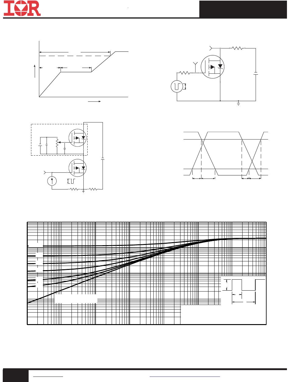
Fig 5. Typical Capacitance Vs.
Drain-to-Source Voltage
Fig 7. Typical Source-Drain Diode
Forward Voltage
Fig 8. Maximum Safe Operating Area
Fig 6. Typical Gate Charge Vs.
Gate-to-Source Voltage
0
20
40
60
80
100
120
140
160
180
1 10 100
C, Capacitance (pF)
DS
-V , Drain-to-Source Voltage (V)
V = 0V, f = 1MHz
C = C + C , C SHORTED
C = C
C = C + C
GS
iss gs gd ds
rss gd
oss ds gd
C
iss
C
oss
C
rss
0
2
4
6
8
10
0.0 1.0 2.0 3.0 4.0
G
GS
-V , Gate-to-Source Voltage (V)
Q , Total Gate Charge (nC)
I = -0.61A
V = -16V
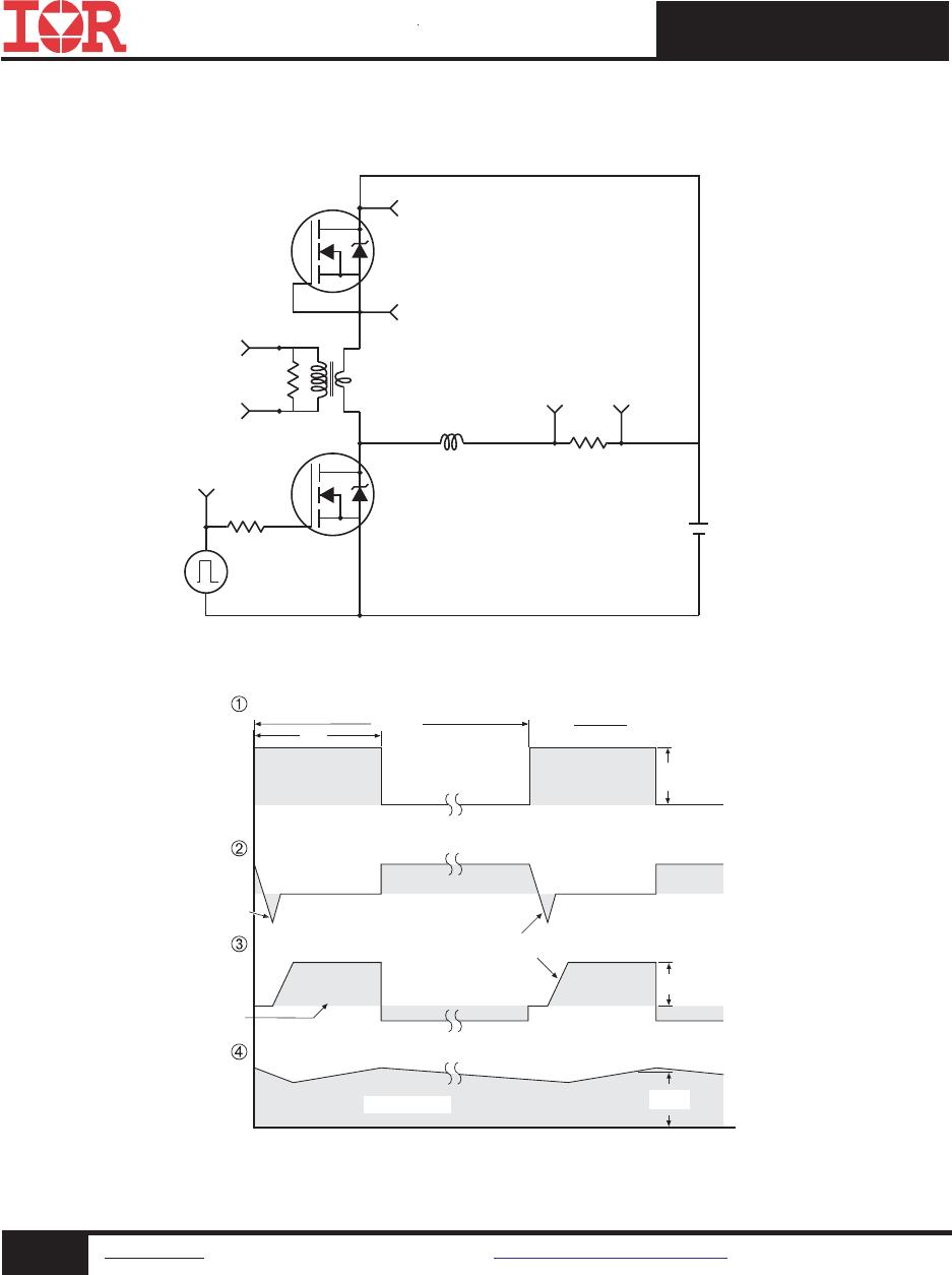
FOR TEST CIRCUIT
SEE FIGURE 9
D
DS
0.01
0.1
1
10
0.4 0.6 0.8 1.0 1.2 1.4
T = 25°C
T = 150°C
J
J
V = 0V
GS
SD
SD
-I , Reverse Drain Current (A)
-V , Source-to-Drain Voltage (V)
0.1
1
10
1 10 100
OPERATION IN THIS AREA LIMITED
BY R
DS(on)
T = 25°C
T = 150°C
Single Pulse
-I , Drain Current (A)
-V , Drain-to-Source Voltage (V)
DS
D
A
J
100μs
1ms
10ms