MP20051 – LOW NOISE HIGH PSRR 1A LINEAR REGULATOR
MP20051 Rev.1.2 www.MonolithicPower.com 3
3/17/2017 MPS Proprietary Information. Patent Protected. Unauthorized Photocopy and Duplication Prohibited.
© 2017 MPS. All Rights Reserved.
PACKAGE REFERENCE
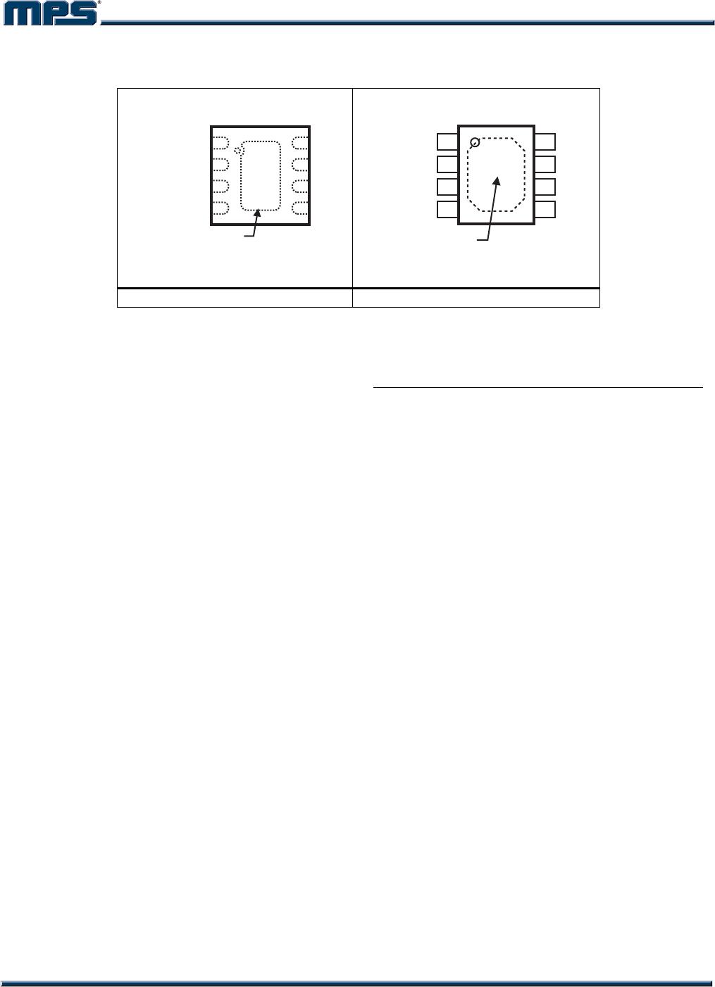
TOP VIEW
OUT
OUT
FB
GND
1
2
3
4
IN
IN
NC
EN
8
7
6
5
EXPOSED PAD
ON BACKSIDE
CONNECT TO GND
OUT
OUT
FB
GND
IN
IN
NC
EN
1
2
3
4
8
7
6
5
TOP VIEW
EXPOSED PAD
ON BACKSIDE
CONNECT TO GND
QFN-8 (3mm x 3mm) SOIC8E
ABSOLUTE MAXIMUM RATINGS
(1)
VIN, EN, FB to GND ....................... -0.3V to +6V
OUT to GND ...................... -0.5V to (V
IN
+ 0.5V)
Continuous Power Dissipation ...... (T
A
=25°C)
(2)
QFN8 (3x3mm)................................................ 2.0W
SOIC8E ............................................................ 2.0W
Junction Temperature ............................... 150C
Storage Temperature Range ..... -65°C to 150°C
Lead Temperature (Soldering, 10sec)........... 260°C
ESD SUSCEPTIBILITY
(3)
HBM (Human Body Mode) .......................... 2kV
MM (Machine Mode) ................................. 200V
Recommended Operating Conditions
(4)
Supply Input Voltage ....................... 2.5V to 5.5V
Enable Input Voltage ......................... 0V to 5.5V
Operating Junction Temp. (T
J
). -40°C to +125°C
Thermal Resistance
(5)
θ
JA
θ
JC
QFN-8 (3mmx3mm) ................ 50 ...... 12 ... °C/W
SOIC8E ................................... 50 ...... 10 ... °C/W
Notes:
1) Exceeding these ratings may damage the device.
2) The maximum allowable power dissipation is a function of the
maximum junction temperature T
J
(MAX), the junction-to-
ambient thermal resistance θ
JA
, and the ambient temperature
T
A
. The maximum allowable continuous power dissipation at
any ambient temperature is calculated by P
D
(MAX) = (T
J
(MAX)-T
A
)/θ
JA
. Exceeding the maximum allowable powe
dissipation will cause excessive die temperature, and the
regulator will go into thermal shutdown. Internal thermal
shutdown circuitry protects the device from permanent
damage.
3) Devices are ESD sensitive. Handling precaution
recommended.
4) The device is not guaranteed to function outside of its
operating conditions.
5) Measured on JESD51-7, 4-layer PCB.