6
Appli cations Information
Introduction
Avago’s HSMS‑286x family of Schottky detector diodes
has been developed specifically for low cost, high
volume designs in two kinds of applications. In small
signal detector applications (P
in
< ‑20 dBm), this diode is
used with DC bias at frequencies above 1.5 GHz. At lower
frequencies, the zero bias HSMS‑285x family should be
considered.
In large signal power or gain control applications
(P
in
> ‑20 dBm), this family is used without bias at
frequencies above 4 GHz. At lower frequencies, the
HSMS‑282x family is preferred.
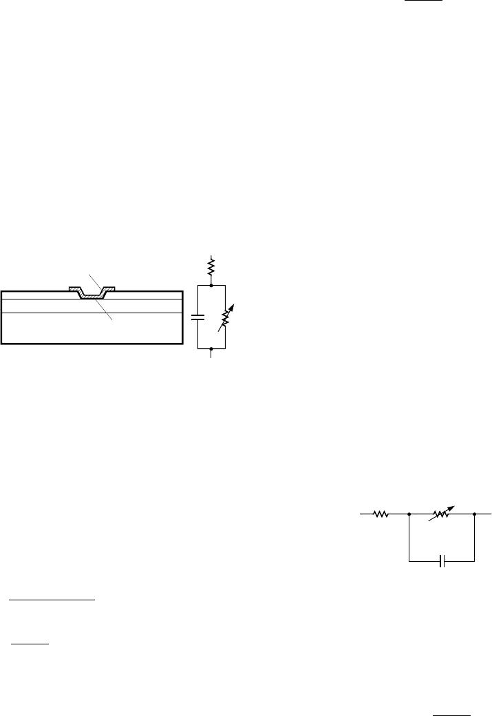
Schottky Barrier Diode Characteristics
Stripped of its package, a Schottky barrier diode chip
consists of a metal‑semiconductor barrier formed by
deposition of a metal layer on a semiconductor. The most
common of several different types, the passivated diode,
is shown in Figure 7, along with its equivalent circuit.
The Height of the Schottky Barrier
The current‑voltage character istic of a Schottky barrier
diode at room temperature is described by the following
equation:
HSMS-285A/6A fig 9
R
S
R
j
C
j
METAL
SCHOTTKY JUNCTION
PASSIVATION PASSIVATION
N-TYPE OR P-TYPE EPI LAYER
N-TYPE OR P-TYPE SILICON SUBSTRATE
CROSS-SECTION OF SCHOTTKY
BARRIER DIODE CHIP
EQUIVALENT
CIRCUIT
Figure 7. Schottky Diode Chip.
R
S
is the parasitic series resistance of the diode, the sum
of the bondwire and leadframe resistance, the resistance
of the bulk layer of silicon, etc. RF energy coupled into
R
S
is lost as heat — it does not contribute to the rectified
output of the diode. C
J
is parasitic junction capaci tance
of the diode, controlled by the thickness of the epitaxial
layer and the diameter of the Schottky contact. R
j
is the
junction resistance of the diode, a function of the total
current flowing through it.
Figure 8. Equivalent Circuit of a Schottky Diode Chip.
R
S
is perhaps the easiest to measure accurately. The V‑I
curve is measured for the diode under forward bias, and
the slope of the curve is taken at some relatively high
value of current (such as 5 mA). This slope is converted
into a resistance R
d
.
8.33 X 10
-5
n T
R
j
= = R
V
- R
s
I
S
+ I
b
0.026
= at 25
°C
I
S
+ I
b
V - IR
S
I = I
S
(exp ( ) - 1)
0.026
8.33 X 10
-5
n T
R
j
= = R
V
- R
s
I
S
+ I
b
0.026
= at 25
°C
I
S
+ I
b
V - IR
S
I = I
S
(exp ( ) - 1)
0.026
where
n = ideality factor (see table of SPICE parameters)
T = temperature in °K
I
S
= saturation current (see table of SPICE parameters)
I
b
= externally applied bias current in amps
I
S
is a function of diode barrier height, and can range
from picoamps for high barrier diodes to as much as 5
µA for very low barrier diodes.
On a semi‑log plot (as shown in the Avago catalog) the
current graph will be a straight line with inverse slope
2.3 X 0.026 = 0.060 volts per cycle (until the effect of R
S
is
seen in a curve that droops at high current). All Schottky
diode curves have the same slope, but not necessar‑
ily the same value of current for a given voltage. This is
deter mined by the saturation current, I
S
, and is related to
the barrier height of the diode.
Through the choice of p‑type or n‑type silicon, and the
selection of metal, one can tailor the characteristics of a
Schottky diode. Barrier height will be altered, and at the
same time C
J
and R
S
will be changed. In general, very
low barrier height diodes (with high values of I
S
, suitable
for zero bias applica tions) are realized on p‑type silicon.
Such diodes suffer from higher values of R
S
than do
the n‑type. Thus, p‑type diodes are generally reserved
for small signal detector applications (where very high
values of R
V
swamp out high R
S
) and n‑type diodes are
used for mixer applications (where high L.O. drive levels
keep R
V
low) and DC biased detectors.
Measuring Diode Linear Parameters
The measurement of the many elements which make
up the equivalent circuit for a pack aged Schottky diode
is a complex task. Various techniques are used for each
element. The task begins with the elements of the diode
chip itself. (See Figure 8).
0.026
R
S
= R
d
-
I
f
For n‑type diodes with relatively low values of saturation
current, C
j
is obtained by measuring the total capaci‑
tance (see AN1124). R
j
, the junction resistance, is calcu‑
lated using the equation given above.