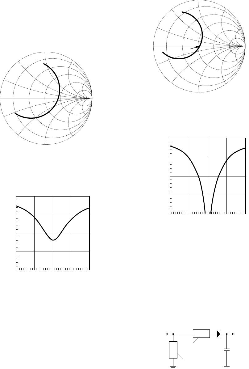
7
The characterization of the surface mount package is
too complex to describe here — linear equivalent circuits
can be found in AN1124.
Detector Circuits (small signal)
When DC bias is available, Schottky diode detector
circuits can be used to create low cost RF and
microwave receivers with a sensitivity of ‑55 dBm to
‑57 dBm.
[1]
Moreover, since external DC bias sets the
video impedance of such circuits, they display classic
square law response over a wide range of input power
levels
[2,3]
. These circuits can take a variety of forms, but
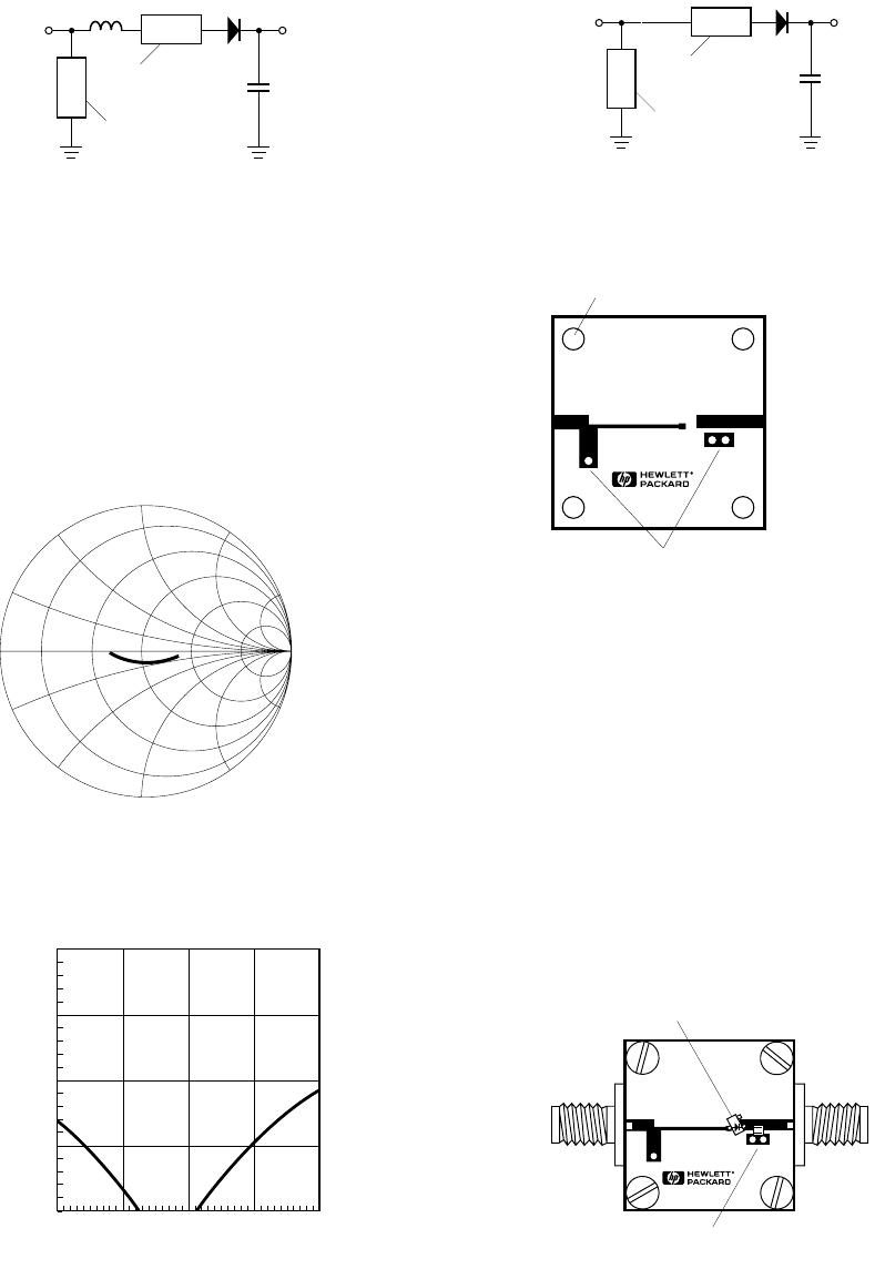
in the most simple case they appear as shown in Figure
9. This is the basic detector circuit used with the HSMS‑
286x family of diodes.
Output voltage can be virtually doubled and input
impedance (normally very high) can be halved through
the use of the voltage doubler circuit
[4]
.
In the design of such detector circuits, the starting point
is the equivalent circuit of the diode. Of interest in the
design of the video portion of the circuit is the diode’s
video impedance — the other elements of the equiv‑
alent circuit disappear at all reasonable video frequen‑
cies. In general, the lower the diode’s video impedance,
the better the design.
The situation is somewhat more complicated in the
design of the RF impedance matching net work, which
includes the pack age inductance and capacitance
(which can be tuned out), the series resistance, the
junction capacitance and the video resistance. Of the
elements of the diode’s equiv alent circuit, the parasitics
are constants and the video resistance is a function of
the current flowing through the diode.
[1]
Avago Application Note 923, Schottky Barrier Diode Video
Detectors.
[2]
Avago Application Note 986, Square Law and Linear Detection.
[3]
Avago Application Note 956‑5, Dynamic Range Extension of Schottky
Detectors.
[4]
Avago Application Note 956‑4, Schottky Diode Voltage Doubler.
[5]
Avago Application Note 963, Impedance Matching Techniques for
Mixers and Detectors.
HSMS-285A/6A fig 12
VIDEO
OUT
RF
IN
Z-MATCH
NETWORK
L
1
DC BIAS
VIDEO
OUT
Z-MATCH
NETWORK
L
1
DC BIAS
RF
IN
Figure 9. Basic Detector Circuits.
HSMS-285A/6A fig 13
1 GHz
2
3
4
5
6
0.2 0.6 1
2
5
Figure 10. RF Impedance of the Diode.
R
V
= R
j
+ R
S
The sum of saturation current and bias current sets
the detection sensitivity, video resistance and input RF
impedance of the Schottky detector diode. Where bias
current is used, some tradeoff in sensitivity and square
law dynamic range is seen, as shown in Figure 5 and
described in reference
[3]
.
The most difficult part of the design of a detector circuit
is the input impedance matching network. For very
broadband detectors, a shunt 60 Ω resistor will give good
input match, but at the expense of detection sensitivity.
When maximum sensitivity is required over a narrow
band of frequencies, a reactive matching network is
optimum. Such net works can be realized in either lumped
or distributed elements, depending upon frequency,
size constraints and cost limitations, but certain general
design principals exist for all types.
[5]
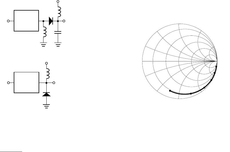
Design work begins
with the RF impedance of the HSMS‑286x series when
bias current is set to 3 µA. See Figure 10.