PMD3001D_2 © NXP B.V. 2009. All rights reserved.
Product data sheet Rev. 02 — 28 August 2009 3 of 16
NXP Semiconductors
PMD3001D
MOSFET driver
5. Limiting values
[1] Device mounted on an FR4 Printed-Circuit Board (PCB), single-sided copper, tin-plated and standard
footprint.
[2] Device mounted on an FR4 PCB, single-sided copper, tin-plated, mounting pad for collector 1cm
2
.
[3] Device mounted on a ceramic PCB, Al
2
O
3
, standard footprint.
Table 5. Limiting values
In accordance with the Absolute Maximum Rating System (IEC 60134).
Symbol Parameter Conditions Min Max Unit
Per transistor; for the PNP transistor with negative polarity
V
CBO
collector-base voltage open emitter - 40 V
V
CEO
collector-emitter voltage open base - 40 V
I
C
collector current - 1 A
I
CM
peak collector current single pulse;
t
p
≤ 1ms
-2A
I
BM
peak base current - 0.3 A
single pulse;
t
p
≤ 1ms
-1A
Per device
P
tot
total power dissipation T
amb
≤ 25 °C
[1]
- 330 mW
[2]
- 400 mW
[3]
- 580 mW
T
j
junction temperature - 150 °C
T
amb
ambient temperature −65 +150 °C
T
stg
storage temperature −65 +150 °C
(1) Ceramic PCB, Al
2
O
3
, standard footprint
(2) FR4 PCB, mounting pad for collector 1cm
2
(3) FR4 PCB, standard footprint
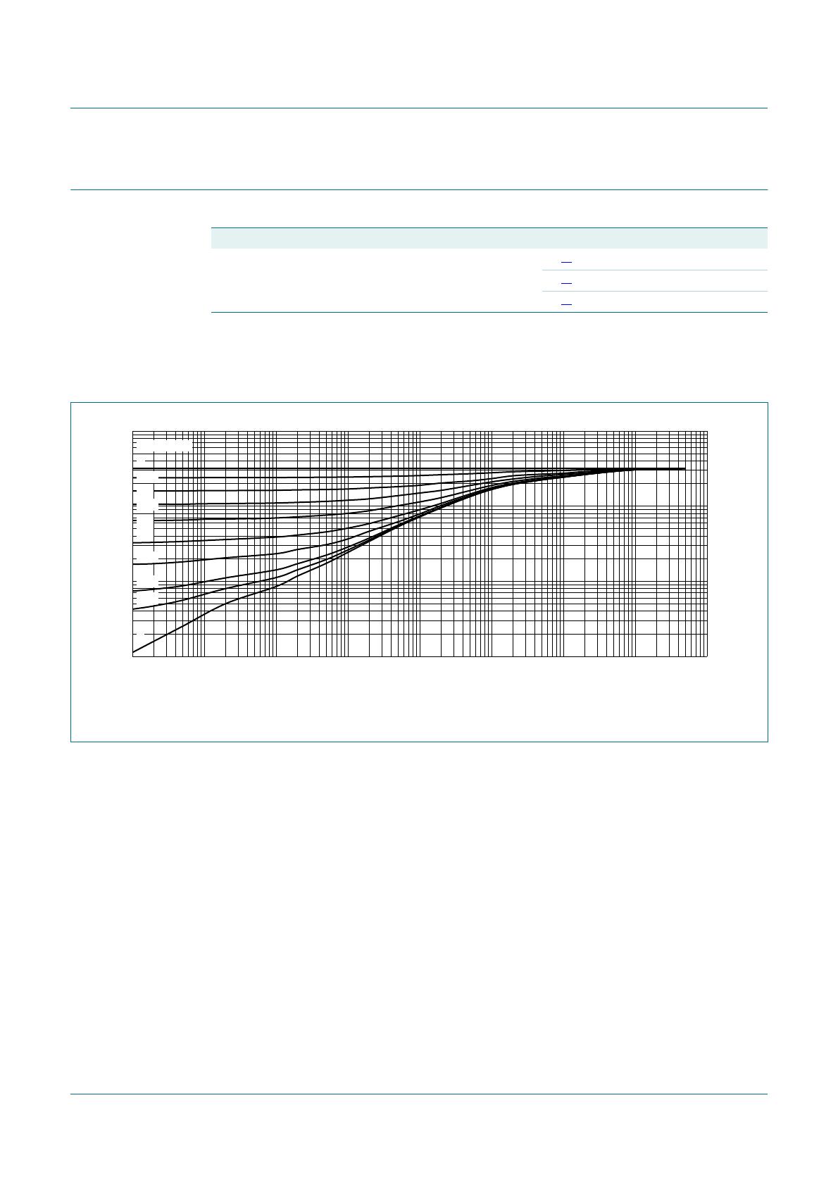
Fig 1. Power derating curves
T
amb
(°C)
−75 17512525 75−25
006aaa784
200
400
600
P
tot
(mW)
0
(1)
(2)
(3)