ADA-4789
Silicon Bipolar Darlington Amplier
Data Sheet
Features
• Small Signal Gain Amplier
• Operating Frequency: DC – 2.5 GHz
• Unconditionally Stable
• 50 Ohms Input & Output
• Flat, Broadband Frequency Response up to 1 GHz
• Operating Current: 40 – 80 mA
• Industry Standard SOT-89 Package
• Single Supply
• VSWR < 2 Throughput Operating Frequency
Specications
900MHz, 3.80V, 60mA (Typical)
• 16.50 dB Associated Gain
• 17.10 dBm P1dB
• 32.60 dBm OIP3
• 4.20 dB Noise Figure
900MHz, 4.10V, 80mA (Typical)
• 16.90 dB Associated Gain
• 18.80 dBm P1dB
• 33.20 dBm OIP3
• 4.30 dB Noise Figure
Applications
• Cellular/PCS/WLL Base Stations
• Wireless Data/WLAN
• Fiber-Optic Systems
• ISM
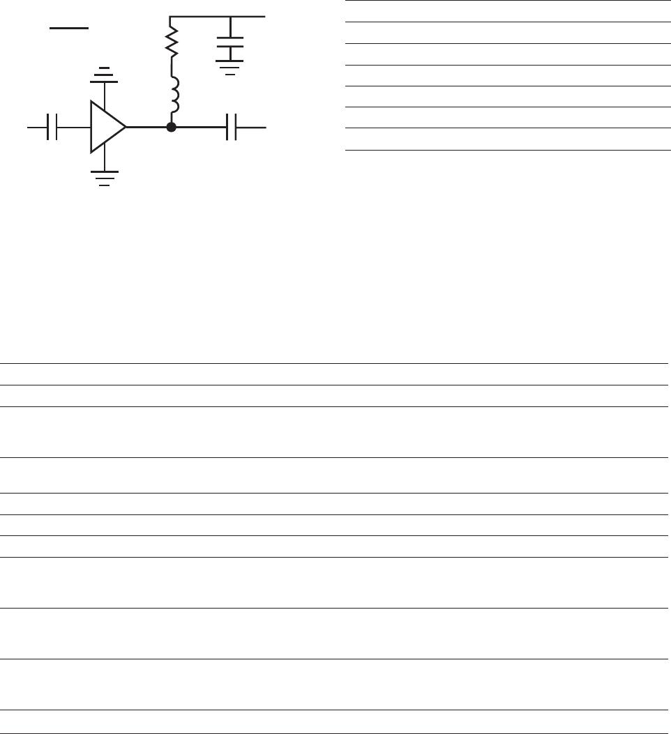
Description
Avago Technologies’ ADA-4789 is an economical, easy-
to-use, general purpose silicon bipolar RFIC gain block
ampliers housed in SOT-89 surface mount plastic pack-
age.
The Darlington feedback structure provides inherent
broad bandwidth performance, resulting in useful oper-
ating frequency up to 2.5 GHz. This is an ideal device for
small-signal gain cascades or IF amplication.
ADA-4789 is fabricated using Avago’s HP25 silicon bi-
polar process, which employs a double-diused single
poly-silicon process with self-aligned submicron emitter
geometry. The process is capable of simultaneous high
fT and high NPN breakdown (25 GHz fT at 6V BVCEO).
The process utilizes industry standard device oxide isola-
tion technologies and submicron aluminum multi-layer
inter-connects to achieve superior performance, high
uniformity, and proven reliability.
Package Marking and Pin Connections
Note: Package marking provides orientation and identication
“4G” = Device Code
“x” = Month code indicates the month of manufacture
4GX
Top View
RFin GND RFout
#1 #2 #3
Bottom View
RFout GND RFin
#3 #2 #1