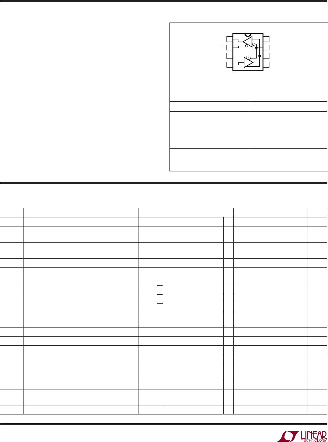
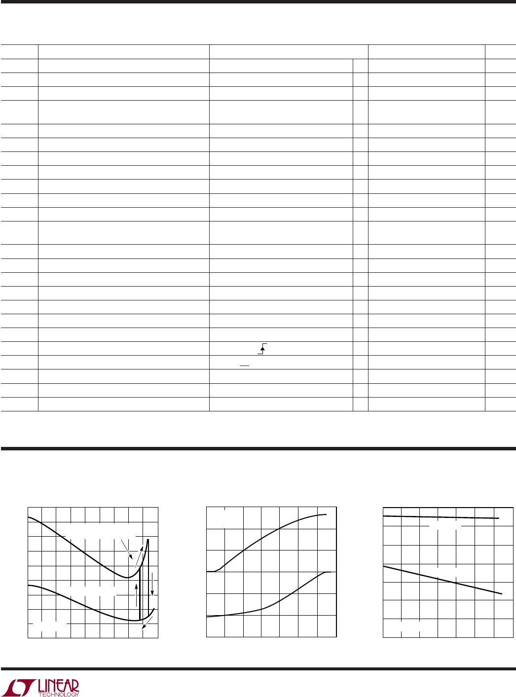
LTC1480IS8#PBF

LTC1480
1
1480fa
OUTPUT CURRENT (mA)
0
0
OUTPUT VOLTAGE (V)
0.5
1.0
1.5
2.0
2.5
60 70 80
1480 TA02
10 20 30 40 50 90
3.0
3.5
V
CC
= 3.3V
T
A
= 25°C
APPLICATIO S
U
DESCRIPTIO
U
FEATURES
TYPICAL APPLICATIO
U
, LTC and LT are registered trademarks of Linear Technology Corporation.
All other trademarks are the property of their respective owners.
True RS485 from a Single 3.3V Supply
Low Power: I
CC
= 500µA Max with Driver Disabled
I
CC
= 600
µ
A Max with Driver Enabled, No Load
1
µ
A Quiescent in Shutdown Mode
–7V to 12V Common Mode Range Permits ±7V
Ground Difference Between Devices on the Data Line
Thermal Shutdown Protection
Power Up/Down Glitch-Free Driver Outputs Permit
Live Insertion or Removal of Transceiver
Driver Maintains High Impedance in Three-State or
with the Power Off
Up to 32 Transceivers on the Bus
50ns Typical Driver Propagation Delays with
10ns Skew
Pin Compatible with the LTC485
Available in 8-Lead DIP and SO Packages
3.3V Ultralow Power
RS485 Transceiver
The LTC
®
1480 is an ultralow power differential line trans-
ceiver which provides full RS485 compatibility while oper-
ating from a single 3.3V supply. It is designed for data
transmission standard RS485 applications with extended
common mode range (12V to –7V). It also meets the
requirements of RS422 and features high speed operation
up to 2.5Mb/s. The CMOS design offers significant power
savings without sacrificing ruggedness against overload
or ESD damage. Typical quiescent current is only 300µA
while operating and 1µA in shutdown.
The driver and receiver feature three-state outputs, with
the driver outputs maintaining high impedance over the
entire common mode range. Excessive power dissipation
caused by bus contention or faults is prevented by a
thermal shutdown circuit which forces the driver outputs
into a high impedance state. The receiver has a fail-safe
feature which guarantees a high output state when the
inputs are left open.
The LTC1480 is fully specified over the commercial and
extended industrial temperature range. The LTC1480 is
available in 8-pin SO and DIP packages.
Battery-Powered RS485/RS422 Applications
Low Power RS485/RS422 Transceiver
Level Translator
Driver Differential
Output Voltage vs Output Current
3.3V RS485 Network
RO
RE
DE
1480 TA01
LTC1480
LTC1480
A
A
B
B
A
B
120120
SHIELD SHIELD
R
3.3V
RO
RE
DE
LTC1480
R
3.3V
3.3V
R
D
RO RE DE DI
D
DI
DI
D
LTC1480
2
1480fa
The denotes the specifications which apply over the full operating
temperature range. V
CC
= 3.3V (Notes 2, 3).
ELECTRICAL CHARACTERISTICS
1
2
3
4
8
7
6
5
TOP VIEW
V
CC
B
A
GND
N8 PACKAGE
8-LEAD PDIP
S8 PACKAGE
8-LEAD PLASTIC SO
R
D
RO
RE
DE
DI
Supply Voltage (V
CC
) ................................................ 7V
Control Input Voltage..................... 0.3V to V
CC
+ 0.3V
Driver Input Voltage....................... 0.3V to V
CC
+ 0.3V
Driver Output Voltage ........................................... ±14V
Receiver Input Voltage.......................................... ±14V
Receiver Output Voltage ................ 0.3V to V
CC
+ 0.3V
Operating Temperature Range
LTC1480C ....................................... 0°C T
A
70°C
LTC1480I.................................... 40°C T
A
85°C
Storage Temperature Range ................. 65°C to 150°C
Lead Temperature (Soldering, 10 sec).................. 300°C
ABSOLUTE AXI U RATI GS
W
WW
U
PACKAGE/ORDER I FOR ATIO
UUW
(Note 1)
T
JMAX
= 125°C,
θ
JA
= 130°C/ W (N8)
T
JMAX
= 125°C,
θ
JA
= 150°C/ W (S8)
ORDER PART NUMBER
S8 PART MARKING
Consult LTC Marketing for parts specified with wider operating temperature ranges.
LTC1480CN8
LTC1480IN8
LTC1480CS8
LTC1480IS8
1480
1480I
Order Options Tape and Reel: Add #TR
Lead Free: Add #PBF Lead Free Tape and Reel: Add #TRPBF
Lead Free Part Marking: http://www.linear.com/leadfree/
SYMBOL PARAMETER CONDITIONS MIN TYP MAX UNITS
V
OD1
Differential Driver Output Voltage (Unloaded) I
O
= 0V 3.3 V
V
OD2
Differential Driver Output Voltage (with Load) R = 27 (RS485) (Figure 1) 1.5 3.3 V
R = 50 (RS422)
2.0 V
V
OD
Change in Magnitude of Driver Differential Output R = 27 or R = 50 (Figure 1) 0.2 V
Voltage for Complementary Output States
V
OC
Driver Common Mode Output Voltage R = 27 or R = 50 (Figure 1) 2V
V
OC
Change in Magnitude of Driver Common Mode R = 27 or R = 50 (Figure 1) 0.2 V
Output Voltage for Complementary Output States
V
IH
Input HIGH Voltage DE, DI, RE 2V
V
IL
Input LOW Voltage DE, DI, RE 0.8 V
I
IN1
Input Current DE, DI, RE ±2 µA
I
IN2
Input Current (A, B) DE = 0, V
CC
= 0V or 3.6V, V
IN
= 12V 1.0 mA
DE = 0, V
CC
= 0V or 3.6V, V
IN
= – 7V 0.8 mA
V
TH
Differential Input Threshold Voltage for Receiver 7V V
CM
12V 0.2 0.2 V
V
TH
Receiver Input Hysteresis V
CM
= 0V 70 mV
V
OH
Receiver Output HIGH Voltage I
O
= – 4mA, V
ID
= 200mV 2V
V
OL
Receiver Output LOW Voltage I
O
= 4mA, V
ID
= – 200mV 0.4 V
I
OZR
Three-State (High Impedance) Output V
CC
= Max, 0.4V V
O
2.4V ±1 µA
Current at Receiver
R
IN
Receiver Input Resistance 7V V
CM
12V 12 k
I
CC
Supply Current No Load, Output Enabled 400 600 µA
No Load, Output Disabled
300 500 µA
I
SHDN
Supply Current in Shutdown Mode DE = 0, RE = V
CC
110µA
LTC1480
3
1480fa
TEMPERATURE (°C)
–40
1.9
2.0
2.2
20 60
1480 G03
1.8
1.7
–20 0
40 80 100
1.6
1.5
2.1
DIFFERENTIAL VOLTAGE (V)
R
L
= 100
R
L
= 54
V
CC
= 3.3V
OUTPUT VOLTAGE (V)
0
OUTPUT CURRENT (mA)
50
100
150
1.5 2.5
1480 G02
0
–50
0.5 1.0
2.0 3.0 3.5
100
150
V
CC
= 3.3V
T
A
= 25°C
TEMPERATURE (°C)
–25
200
SUPPLY CURRENT (µA)
225
275
300
325
75
425
1480 G01
250
25 175125
–50
50
0 150100
350
375
400
DRIVER DISABLED
THERMAL SHUTDOWN
WITH DRIVER ENABLED
V
CC
= 3.3V
The denotes the specifications which apply over the full operating
temperature range. V
CC
= 3.3V (Notes 2, 3).
TYPICAL PERFOR A CE CHARACTERISTICS
UW
Note 1: Absolute maximum ratings are those beyond which the safety of
the device cannot be guaranteed.
Note 2: All currents into device pins are positive; all currents out ot device pins
are negative. All voltages are referenced to device ground unless otherwise specified.
Note 3: All typicals are given for V
CC
= 3.3V and T
A
= 25°C.
Driver Output Low/High Voltage
vs Output Current
Supply Current vs Temperature
Driver Differential Output Voltage
vs Temperature
SWITCHI G CHARACTERISTICS
U
SYMBOL PARAMETER CONDITIONS MIN TYP MAX UNITS
I
OSD1
Driver Short-Circuit Current, V
OUT
= HIGH 7V V
O
12V 35 250 mA
I
OSD2
Driver Short-Circuit Current, V
OUT
= LOW 7V V
O
12V 35 250 mA
I
OSR
Receiver Short-Circuit Current 0V V
O
V
CC
785mA
t
PLH
Driver Input to Output R
DIFF
= 54, C
L1
= C
L2
= 100pF, 25 50 80 ns
(Figures 3, 5)
t
PHL
Driver Input to Output 25 50 80 ns
t
SKEW
Driver Output to Output 10 20 ns
t
R
, t
F
Driver Rise or Fall Time 51540ns
t
ZH
Driver Enable to Output HIGH C
L
= 100pF (Figures 4, 6), S2 Closed 70 120 ns
t
ZL
Driver Enable to Output LOW C
L
= 100pF (Figures 4, 6), S1 Closed 70 120 ns
t
LZ
Driver Disable Time from LOW C
L
= 15pF (Figures 4, 6), S1 Closed 70 120 ns
t
HZ
Driver Disable Time from HIGH C
L
= 15pF (Figures 4, 6), S2 Closed 70 120 ns
t
PLH
Receiver Input to Output R
DIFF
= 54, C
L1
= C
L2
= 100pF, 30 140 200 ns
(Figures 3, 7)
t
PHL
Receiver Input to Output 30 140 200 ns
t
SKD
t
PLH
– t
PHL
Differential Receiver Skew 13 ns
t
ZL
Receiver Enable to Output LOW C
RL
= 15pF (Figures 2, 8), S1 Closed 50 80 ns
t
ZH
Receiver Enable to Output HIGH C
RL
= 15pF (Figures 2, 8), S2 Closed 50 80 ns
t
LZ
Receiver Disable from LOW C
RL
= 15pF (Figures 2, 8), S1 Closed 50 80 ns
t
HZ
Receiver Disable from HIGH C
RL
= 15pF (Figures 2, 8), S2 Closed 50 80 ns
f
MAX
Maximum Data Rate 2.5 Mbits/s
t
SHDN
Time to Shutdown DE = 0, RE = 50 200 600 ns
t
ZH(SHDN)
Driver Enable from Shutdown to Output HIGH C
L
= 100pF (Figures 4, 6), S2 Closed 70 120 ns
t
ZL(SHDN)
Driver Enable from Shutdown to Output LOW C
L
= 100pF (Figures 4, 6), S1 Closed 70 120 ns
t
ZH(SHDN)
Receiver Enable from Shutdown to Output HIGH C
L
= 15pF (Figures 2, 8), S2 Closed 4500 ns
t
ZL(SHDN)
Receiver Enable from Shutdown to Output LOW C
L
= 15pF (Figures 2, 8), S1 Closed 4500 ns

LTC1480IS8#PBF

Mfr. #:
Manufacturer:
Analog Devices Inc.
Description:
RS-485 Interface IC 3.3V Ultralow Pwr RS485 Tran
Lifecycle:
New from this manufacturer.
Delivery:
DHL FedEx Ups TNT EMS
Payment:
T/T Paypal Visa MoneyGram Western Union