LTC1480IS8#PBF

LTC1480
4
1480fa
TEMPERATURE (°C)
–40
2.0
OUTPUT VOLTAGE (V)
2.4
3.0
0
40
60
1480 G09
2.2
2.8
2.6
–20
20
80
100
V
CC
= 3.3V
I
O
= 8mA
TEMPERATURE (°C)
–40
OUTPUT VOLTAGE (V)
0.4
0.5
0.6
20 60
1480 G08
0.3
0.2
–20 0
40 80 100
0.1
0
V
CC
= 3.3V
I
O
= 8mA
PI FU CTIO S
UU U
TEMPERATURE (°C)
–40
TIME (ns)
12
10
8
6
4
2
0
20 60
1480 G07
–20 0
40 80 100
V
CC
= 3.3V
OUTPUT VOLTAGE (V)
3.30
OUTPUT CURRENT (mA)
–8
–10
–12
1.30
1480 G06
–6
–4
0
2.80
2.30
1.80
–2
–16
–14
3.05
2.55
2.05
1.55
V
CC
= 3.3V
T
A
= 25°C
OUTPUT VOLTAGE (V)
0
OUTPUT CURRENT (mA)
15
20
25
1.6
1480 G05
10
5
0
0.2 0.4 0.6 1.0 1.4 1.8
0.8
1.2
2.0
V
CC
= 3.3V
T
A
= 25°C
TEMPERATURE (°C)
–40
TIME (ns)
6.5
20
1480 G04
5.0
4.0
–20 0 40
3.5
3.0
7.0
6.0
5.5
4.5
60 80 100
V
CC
= 3.3V
TYPICAL PERFORMANCE CHARACTERISTICS
U
W
high, the driver outputs will be fed back to the receiver and
the receive output will correspond to the driver input.
DI (Pin 4): Driver Input. If the driver outputs are enabled
(DE HIGH) then a low on DI forces the outputs A LOW and
B HIGH. A HIGH on DI with the driver outputs enabled will
force A HIGH and B LOW.
GND (Pin 5): Ground.
A (Pin 6): Driver Output/Receiver Input.
B (Pin 7): Driver Output/Receiver Input.
V
CC
(Pin 8): Positive Supply. 3.0V < V
CC
< 3.6V.
RO (Pin 1): Receiver Output. If the receiver output is
enabled (RE LOW) and A > B by 200mV, then RO will be
HIGH. If A < B by 200mV, then RO will be LOW.
RE (Pin 2): Receiver Output Enable. A LOW enables the
receiver output, RO. A HIGH input forces the receiver
output into a high impedance state.
DE (Pin 3): Driver Outputs Enable. A HIGH on DE enables
the driver output. A, B and the chip will function as a line
driver. A low input will force the driver outputs into a high
impedance state and the chip will function as a line
receiver. If RE is high and DE is LOW, the part will enter a
low power (1µA) shutdown state. If RE is low and DE is
Receiver Output Low Voltage
vs Output Current
Receiver Output High Voltage
vs Output Current
Driver Skew vs Temperature
Receiver
t
PLH
– t
PHL
vs Temperature
Receiver Output Low Voltage
vs Temperature
Receiver Output High Voltage
vs Temperature
LTC1480
5
1480fa
DI
3V
1.5V
t
PLH
t
r
t
SKEW
1/2 V
O
V
O
f = 1MHz, t
r
10ns, t
f
10ns
90%
10%
0V
B
A
V
O
–V
O
0V
90%
1.5V
t
PHL
t
SKEW
1/2 V
O
10%
t
f
V
DIFF
= V(A) – V(B)
1480 F05
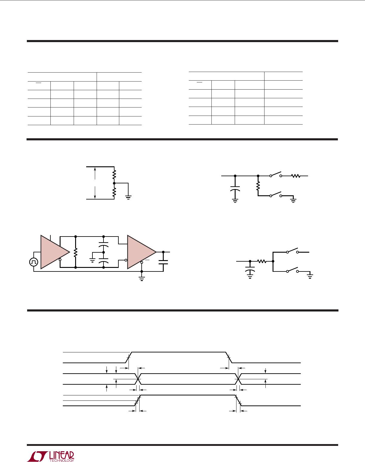
SWITCHI G TI E WAVEFOR S
UW W
OUTPUT
UNDER TEST
C
L
S1
S2
V
CC
500
1480 F04
3V
DE
A
B
DI
R
DIFF
C
L1
C
L2
RO
15pF
A
B
RE
1480 F03
LTC1480
RECEIVER
LTC1480
DRIVER
RECEIVER
OUTPUT
C
RL
1k
S1
S2
TEST POINT
V
CC
1k
1480 F02
V
OD
A
B
R
R
V
OC
1480 F01
TEST CIRCUITS
FU CTIO TABLES
UU
LTC1480 Transmitting
INPUTS OUTPUTS
RE DE DI B A
X1101
X1010
00XZZ
1 0 X Z* Z*
*Shutdown mode
LTC1480 Receiving
INPUTS OUTPUTS
RE DE A – B RO
000.2V 1
00 0.2V 0
0 0 Inputs Open 1
10 X Z*
*Shutdown mode
Figure 2. Receiver Timing Test Load
Figure 1. Driver DC Test Load
Figure 5. Driver Propagation Delays
Figure 4. Driver Timing Test Load
Figure 3. Driver/Receiver Timing Test Circuit
LTC1480
6
1480fa
LOGIC
V
CC
SD3
P1
D1
OUTPUT
SD4
D2
N1
1480 F10
P1
LOGIC
V
CC
P1
D1
OUTPUT
D2
N1
1480 F09
1.5V
t
ZL(SHDN)
, t
ZL
t
ZH(SHDN)
, t
ZH
1.5V
1.5V
1.5V
t
LZ
0.5V
0.5V
t
HZ
OUTPUT NORMALLY LOW
OUTPUT NORMALLY HIGH
3V
0V
RE
3.3V
V
OL
V
OH
0V
RO
RO
1480 F08
f = 1MHz, t
r
10ns, t
f
10ns
1.5V
t
PHL
RO
–V
OD2
A – B
0V 0V
1.5V
t
PLH
OUTPUT
INPUT
V
OD2
V
OL
V
OH
1480 F07
f = 1MHz, t
r
10ns, t
f
10ns
1.5V
2.3V
2.3V
t
ZH(SHDN)
,
t
ZH
t
ZL(SHDN)
,
t
ZL
1.5V
t
LZ
0.5V
0.5V
t
HZ
OUTPUT NORMALLY LOW
OUTPUT NORMALLY HIGH
3V
0V
DE
3.3V
V
OL
V
OH
0V
A, B
A, B
1480 F06
f = 1MHz, t
r
10ns, t
f
10ns
APPLICATIO S I FOR ATIO
WUU
U
SWITCHI G TI E WAVEFOR S
UW W
CMOS Output Driver
The LTC1480 transceiver provides full RS485 compatibility
while operating from a single 3.3V supply. The RS485
specification requires that a transceiver withstand common
mode voltages of up to 12V or –7V at the RS485 line
connections. Additionally, the transceiver must be immune
to both ESD and latch-up. This rules out traditional CMOS
drivers, which include parasitic diodes from their driver
outputs to each supply rail (Figure 9). The LTC1480 uses a
proprietary process enhancement which adds a pair of
Schottky diodes to the output stage (Figure 10), preventing
Figure 9. Conventional
CMOS Output Stage
Figure 10.
LTC1480 Output Stage
Figure 6. Driver Enable and Disable Times
Figure 7. Receiver Propagation Delays
Figure 8. Receiver Enable and Disable Times

LTC1480IS8#PBF

Mfr. #:
Manufacturer:
Analog Devices Inc.
Description:
RS-485 Interface IC 3.3V Ultralow Pwr RS485 Tran
Lifecycle:
New from this manufacturer.
Delivery:
DHL FedEx Ups TNT EMS
Payment:
T/T Paypal Visa MoneyGram Western Union