2
CGHV40320D Rev 0.0
Cree, Inc.
4600 Silicon Drive
Durham, North Carolina, USA 27703
USA Tel: +1.919.313.5300
Fax: +1.919.869.2733
www.cree.com/rf
Copyright © 2014 Cree, Inc. All rights reserved. The information in this document is subject to change without notice. Cree and the
Cree logo are registered trademarks of Cree, Inc. Other trademarks, product and company names are the property of their respective
owners and do not imply specic product and/or vendor endorsement, sponsorship or association.
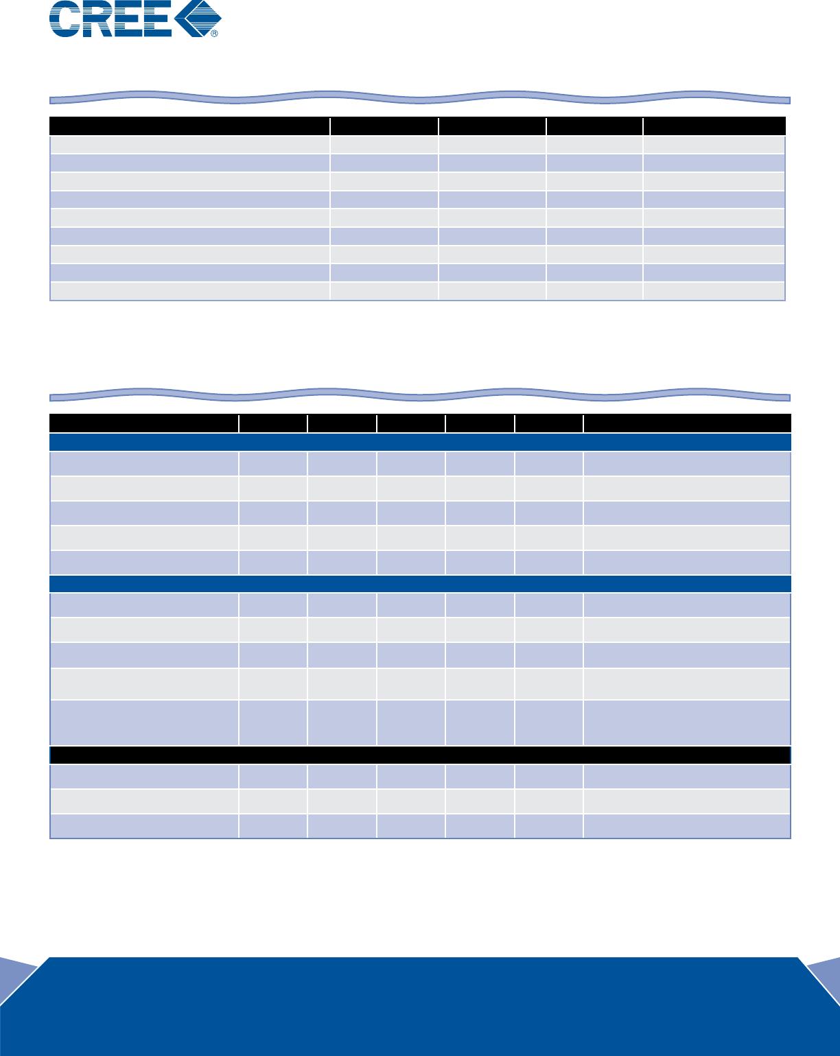
Absolute Maximum Ratings (not simultaneous)
Parameter Symbol Rating Units Conditions
Drain-source Voltage V
DSS
150 V
DC
25˚C
Gate-source Voltage V
GS
-10, +2 V
DC
25˚C
Storage Temperature T
STG
-65, +150 ˚C
Operating Junction Temperature T
J
225 ˚C
Maximum Drain Current
1
I
MAX
12 A 25˚C
Maximum Forward Gate Current I
GMAX
41.8 mA 25˚C
Thermal Resistance, Junction to Case (packaged)
2
R
θJC
0.44 ˚C/W 85˚C,167.2WDissipation
Thermal Resistance, Junction to Case (die only) R
θJC
0.35 ˚C/W 85˚C,167.2WDissipation
Mounting Temperature T
S
320 ˚C 30 seconds
Note
1
Current limit for long term reliable operation.
Note
2
Eutecticdieattachusing80/20AuSnmountedtoa10milthickCu15Mo85carrier.
Electrical Characteristics (Frequency = 4 GHz unless otherwise stated; T
C
= 25˚C)
Characteristics Symbol Min. Typ. Max. Units Conditions
DC Characteristics
Gate Pinch-Off Voltage V
P
-3.8 -3.0 –2.3 V V
DS
= 10 V, I
D
= 41.8 mA
Drain Current
1
I
DSS
33 41.8 – A V
DS
= 6 V, V
GS
= 2.0 V
Drain-Source Breakdown Voltage V
BD
150 – – V V
GS
= -8 V, I
D
= 41.8 mA
On Resistance R
ON
– 0.07 – Ω V
DS
= 0.1 V
Gate Forward Voltage V
G-ON
– 1.9 – V I
GS
= 41.8 mA
RF Characteristics
Small Signal Gain G
SS
– 19 – dB V
DD
= 50 V, I
DQ
= 500 mA
Saturated Power Output
2
P
SAT
– 320 – W V
DD
= 50 V, I
DQ
= 500 mA
DrainEfciency
3
η
– 65 – % V
DD
= 50 V, I
DQ
= 500 mA, P
SAT
= 320 W
Intermodulation Distortion IM3 – -30 – dBc
V
DD
= 50 V, I
DQ
= 500 mA,
P
OUT
= 320 W PEP
Output Mismatch Stress VSWR – – 10 : 1
Y
No damage at all phase angles,
V
DD
= 50 V, I
DQ
= 500 mA,
P
OUT
= 320 W Pulsed
Dynamic Characteristics
Input Capacitance C
GS
– 55.6 – pF V
DS
= 50 V, V
gs
= -8 V, f = 1 MHz
Output Capacitance C
DS
– 11.56 – pF V
DS
= 50 V, V
gs
= -8 V, f = 1 MHz
Feedback Capacitance C
GD
– 1.23 – pF V
DS
= 50 V, V
gs
= -8 V, f = 1 MHz
Notes:
1
Scaled from PCM data
2
P
SAT
isdenedasI
G
= 4.0 mA.
3
DrainEfciency=P
OUT
/P
DC