LTC4231
13
4321fa
For more information www.linear.com/LTC4231
applicaTions inForMaTion
Auto-Retry vs Latchoff
During current fault mode, GATE is held low and TIMER is
discharged to GND. Once TIMER < 0.1V, average I
CC
goes
to 4µA and the internal current fault latch is ready to be
reset. The LTC4231-2 (automatic retry) waits for a 500ms
retry delay after which the internal current fault latch is
reset and GATE ramps up to turn the MOSFET back on.
The LTC4231-1 (latchoff) version does not restart automati
-
cally. Pulling SHDN low for >100µs will reset the internal
current fault latch. When SHDN goes high, GATE ramps
up after a debounce cycle. Alternatively, IN can be pulled
to GND for >100µs then cycled back up again. This UVLO
event will reset the internal current fault latch and GATE
ramps up after a debounce cycle. A UV/OV detected at IN
also resets the internal current fault latch and GATE ramps
up after a debounce delay.
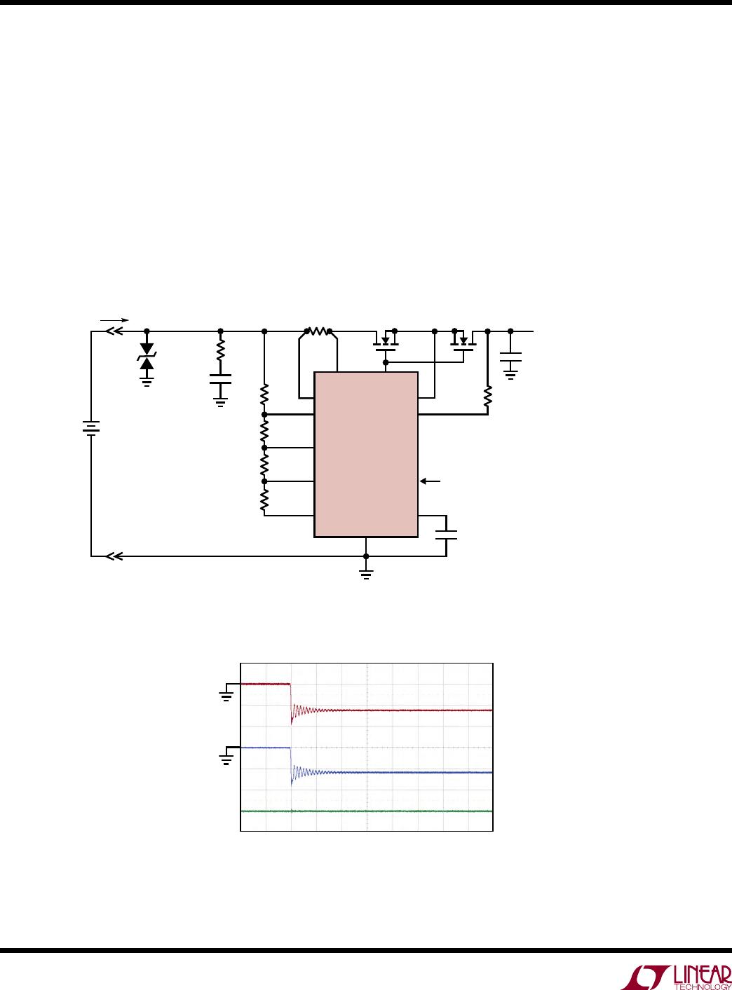
Analog Current Limit Loop Stability
The analog current limit loop on GATE is compensated by
the parasitic gate capacitance of the external MOSFET. No
further compensation components are normally required.
If a small MOSFET with C
ISS
≤ 1nF is chosen, an R
G
and
C
G
compensation network connected at GATE may be
required (Figure 1) to ensure stability. The resistor, R
G
,
connected in series with C
G
accelerates the MOSFET gate
recovery after a fast gate pull-down. The value of C
G
should
be ≤100nF. An additional 10Ω resistor (R5 in Figure 1)
should be added close to the MOSFET gate to prevent
possible parasitic oscillation due to trace/wire inductance
and capacitance.
Monitor OV and UV Faults
When IN is above UVLO and SHDN is high, an internal
clock times a 200µs strobe of the resistive divider at IN
every 10ms. During this 200µs strobe, the normally high
impedance GNDSW is connected to GND with an internal
80Ω switch and the comparators connected to UVH, UVL
and OV are awakened from sleep mode. The comparators
sense the voltages on the resistive divider, and their outputs
are latched at the end of the strobe window.
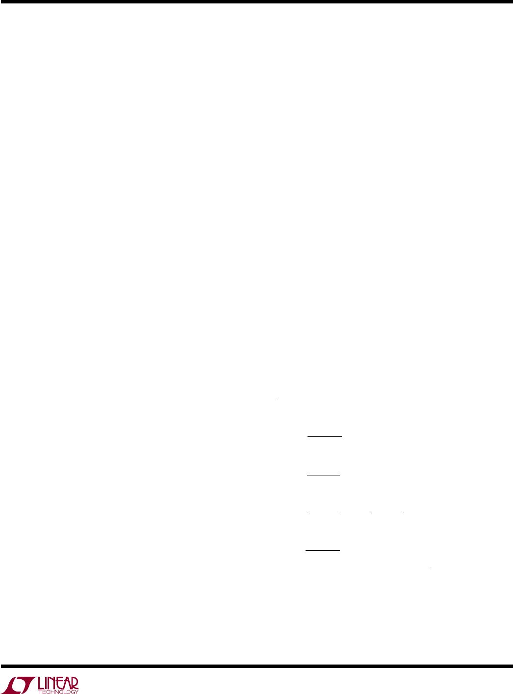
If an OV or UV violation is detected, the STATUS pulls
low and a 1mA pull-down will be activated between GATE
and GND to turn off the external MOSFET. When GATE
goes <1.2V, average I
CC
drops to 4µA as the LTC4231
goes into voltage fault mode. It stays in this mode until a
subsequent IN
strobe sees no OV/UV. The LTC4231 then
re-starts after a debounce cycle.
Strobing the resistive divider reduces power consumption
as the external resistors as well as the internal OV/UV
comparators do not dissipate power in between strobes.
For a 1M string of resistors used to monitor a V
IN
of 24V,
this strobing scheme reduces the current consumption
from 24µA to 0.48µA as the strobing duty cycle is 2%
(200µs/10ms). The OV/UV comparators dissipate 35µA
during IN strobing. The 2% duty cycle reduces this to an
average current of 0.7µA. Note that the response time to
an OV/UV event can be as long as 10ms.
The four resistors allow three thresholds to be configured.
They are the UV rising threshold (V
UVON
), the UV falling
threshold (V
UVOFF
) and the OV rising threshold (V
OVOFF
).
The OV falling threshold is set by internal hysteresis to be
1.8% below the OV rising threshold. Using the compara
-
tor threshold as 0.795V and choosing appropriate values
for R
TOTAL
and R4, the resistor values can be calculated
as follows:
TOTAL
R4 =
0.795V
V
OVOFF
•R
TOTAL
R3 =
V
OVOFF
V
UVON
− 1
•R4
R2 =
V
UVON
V
UVOFF
− 1
•
V
OVOFF
V
UVON
•R4
R1=
U
OVOFF
0.795V
− 1
•R4−R3− R2
It is recommended that the total value of the resistor
string be less than 2M and traces at UVH, UVL, and OV
kept short to minimize parasitic capacitance and improve
settling time.