AT-32033-TR1G

AT-32011, AT-32033
Low Current, High Performance NPN
Silicon Bipolar Transistor
Data Sheet
Description
Avagos AT-32011 and AT-32033 are high performance
NPN bipolar transistors that have been optimized for
maximum f
t
at low voltage operation, making them ideal
for use in battery powered applications in wireless mar-
kets. The AT-32033 uses the 3 lead SOT-23, while the AT-
32011 places the same die in the higher performance 4
lead SOT-143. Both packages are industry standard, and
compatible with high volume surface mount assembly
techniques.
The 3.2 micron emitter-to-emitter pitch and reduced
parasitic design of these transistors yields extremely high
performance products that can perform a multiplicity
of tasks. The 20 emitter nger interdigitated geometry
yields an easy to match to and extremely fast transistor
with moderate power, low noise resistance, and low op-
erating currents.
Optimized performance at 2.7 V makes these devices
ideal for use in 900 MHz, 1.8 GHz, and 2.4 GHz battery
operated systems as an LNA, gain stage, buer, oscilla-
tor, or active mixer. Typical amplier designs at 900 MHz
yield 1.2 dB noise gures with 12 dB or more associated
gain at a 2.7 V, 2 mA bias, with noise performance being
relatively insensitive to input match. High gain capabil-
ity at 1 V, 1 mA makes these devices a good t for 900
MHz pager applications. Voltage breakdowns are high
enough for use at 5 volts.
The AT-3 series bipolar transistors are fabricated using
an optimized version of Avagos 10 GHz f
t
, 30 GHz f
MAX
Self-Aligned-Transistor (SAT) process. The die are nitride
passivated for surface protection. Excellent device uni-
formity, performance and reliability are produced by the
use of ion-implantation, self-alignment techniques, and
gold metalization in the fabrication of these devices.
Features
High Performance Bipolar Transistor Optimized for
Low Current, Low Voltage Operation
900 MHz Performance:
AT-32011: 1 dB NF, 14 dB G
A
AT-32033: 1 dB NF, 12.5 dB G
A
Characterized for End-Of-Life Battery Use (2.7 V)
SOT-23 and SOT-143 SMT Plastic Packages
Tape-And-Reel Packaging Option Available
Lead-free
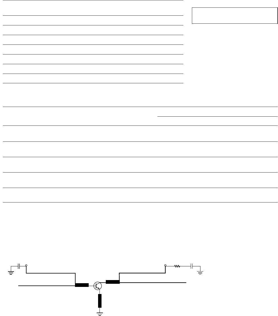
Pin Connections and Package Marking
Notes:
Top View. Package Marking provides orientation and identication.
"x" is the date code.
BASE EMITTER
EMITTER COLLECTOR
BASE EMITTER
COLLECTOR
320x
320x
SOT-23 (AT-32033)
SOT-143 (AT-32011)
Note:
Top view. Package marking provides orientation
and identification. "x" is the date code.
2
AT-32011, AT-32033 Absolute Maximum Ratings
Absolute
Symbol Parameter Units Maximum
[1]
V
EBO
Emitter-Base Voltage V 1.5
V
CBO
Collector-Base Voltage V 11
V
CEO
Collector-Emitter Voltage V 5.5
I
C
Collector Current mA 32
P
T
Power Dissipation
[2, 3]
mW 200
T
j
Junction Temperature °C 150
T
STG
Storage Temperature °C -65 to 150
Electrical Specications, T
A
= 25°C
AT-32011 AT-32033
Symbol Parameters and Test Conditions Units Min. Typ. Max. Min. Typ. Max.
NF Noise Figure
V
CE
= 2.7 V, I
C
= 2 mA f = 0.9 GHz dB 1.0
[1]
1.3
[1]
1.0
[2]
1.3
[2]
G
A
Associated Gain
V
CE
= 2.7 V, I
C
= 2 mA f = 0.9 GHz dB 12.5
[1]
14
[1]
11
[2]
12.5
[2]
h
FE
Forward Current Transfer Ratio
V
CE
= 2.7 V, I
C
= 2 mA 70 300 70 300
I
CBO
Collector Cuto Current
V
CB
= 3 V µA 0.2 0.2
I
EBO
Emitter Cuto Current
V
EB
= 1 V µA 1.5 1.5
Notes:
1. Test circuit A, Figure 1. Numbers reect device performance de-embedded from circuit losses. Input loss = 0.3 dB;
output loss = 0.3 dB.
2. Test circuit B, Figure 1. Numbers reect device performance de-embedded from circuit losses. Input loss = 0.3 dB;
output loss = 0.3 dB.
Thermal Resistance
[2]
:
θ
jc
= 550 °C/W
Notes:
1. Operation of this device above any one
of these parameters may cause permanent
damage.
2. T
Mounting Surface
= 25°C.
3. Derate at 1.82 mW/°C for T
C
> 40°C.
AT-32011 fig 1
1000 pF
V
BB
W = 10 L = 1870
W = 10
CKT A: L = 380
CKT B: L = 380
W = 30
L = 60
W = 10 L = 1870
1000 pF
V
CC
W = 10
CKT A: L = 105
CKT B: L = 850
CKT A: W = 30 L = 50 x 2
CKT B: W = 30 L = 60
TEST CIRCUIT
BOARD MATL = 0.062" FR-4 (ε = 4.8)
RF IN
W = 30
L = 60
CKT A: 25
CKT B: 5
RF OUT
NOT TO SCALE
DIMENSIONS IN MILS
Figure 1. Test Circuit for Noise Figure and Associated Gain.
This circuit is a compromise match between best noise gure, best gain, stability, and a practical synthesizable match.
3
Characterization Information, T
A
= 25°C
AT-32011 AT-32033
Symbol Parameters and Test Conditions Units Typ. Typ.
P
1dB
Power at 1 dB Gain Compression (opt tuning)
V
CE
= 2.7 V, I
C
= 20 mA f = 0.9 GHz dBm 13 13
G
1dB
Gain at 1 dB Gain Compression (opt tuning)
V
CE
= 2.7 V, I
C
= 20 mA f = 0.9 GHz dB 16.5 15
IP
3
Output Third Order Intercept Point (opt tuning)
V
CE
= 2.7 V, I
C
= 20 mA f = 0.9 GHz dBm 24 24
|S
21
|
E
2
Gain in 50 Ω System
V
CE
= 2.7 V, I
C
= 2 mA f = 0.9 GHz dB 13 11.5
AT-32011 fig 2
NOISE FIGURE (dB)
0
0
FREQUENCY (GHz)
1 1.5
2
1
0.5
0.5 2.5
1.5
2
1 mA
2 mA
5 mA
10 mA
20 mA
AT-32011 fig 3
Ga (dB)
0
0
FREQUENCY (GHz)
1.0 1.5
25
10
5
0.5 2.5
15
2.0
20
1 mA
2 mA
5 mA
10 mA
20 mA
AT-32011 fig 4
Ga (dB)
0
0
FREQUENCY (GHz)
1.0 1.5
10
5
0.5 2.5
15
2.0
20
1 mA
2 mA
5 mA
10 mA
20 mA
Figure 4. AT-32033 Associated Gain at Optimum Noise
Match vs. Frequency and Current at V
CE
= 2.7 V.
Figure 2. AT-32011 and AT-32033 Minimum Noise Fig-
ure vs. Frequency and Current at V
CE
= 2.7 V.
Figure 3. AT-32011 Associated Gain at Optimum Noise
Match vs. Frequency and Current at V
CE
= 2.7 V.
Figure 6. AT-32011 1 dB Compressed Gain vs. Frequen-
cy and Current at V
CE
= 2.7 V.
Figure 5. AT-32011 and AT-32033 Power at 1 dB Gain
Compression vs. Frequency and Current at V
CE
= 2.7 V.
Figure 7. AT-32033 1 dB Compressed Gain vs. Frequen-
cy and Current at V
CE
= 2.7 V.
AT-32011 fig 5
P 1dB (dBm)
0
-5
FREQUENCY (GHz)
1.0 1.5
20
5
0
0.5 2.5
10
2.0
15
2 mA
5 mA
10 mA
20 mA
AT-32011 fig 6
G 1dB (dB)
0
0
FREQUENCY (GHz)
1.0 1.5
20
10
5
0.5 2.5
15
2.0
2 mA
5 mA
10 mA
20 mA
AT-32011 fig 7
G 1dB (dB)
0
0
FREQUENCY (GHz)
1.0 1.5
20
10
5
0.5 2.5
15
2.0
2 mA
5 mA
10 mA
20 mA

AT-32033-TR1G

Mfr. #:
Manufacturer:
Broadcom / Avago
Description:
RF Bipolar Transistors Transistor Si Low Current
Lifecycle:
New from this manufacturer.
Delivery:
DHL FedEx Ups TNT EMS
Payment:
T/T Paypal Visa MoneyGram Western Union