6
AT-32011 Typical Scattering Parameters, Common Emitter, Zo = 50 Ω, V
CE
= 2.7 V, I
C
= 2 mA
Freq. S
11
S
21
S
12
S
22
GHz Mag Ang dB Mag Ang dB Mag Ang Mag Ang
0.1 0.94 -13 16.67 6.81 170 -35.25 0.017 82 0.99 -6
0.5 0.80 -60 15.10 5.69 136 -23.07 0.070 57 0.86 -24
0.9 0.67 -97 12.97 4.45 112 -20.34 0.096 41 0.73 -35
1.0 0.64 -104 12.48 4.21 107 -20.05 0.099 39 0.70 -37
1.5 0.55 -137 10.04 3.18 86 -19.21 0.110 30 0.61 -45
1.8 0.51 -154 8.77 2.75 76 -19.04 0.112 28 0.58 -49
2.0 0.50 -165 8.13 2.55 70 -18.99 0.112 27 0.56 -52
2.4 0.48 176 6.75 2.18 58 -18.84 0.114 27 0.54 -57
3.0 0.49 150 4.97 1.77 43 -18.52 0.119 30 0.52 -64
4.0 0.54 116 2.73 1.37 22 -16.98 0.142 36 0.50 -77
5.0 0.61 92 0.83 1.10 4 -14.50 0.188 37 0.50 -95
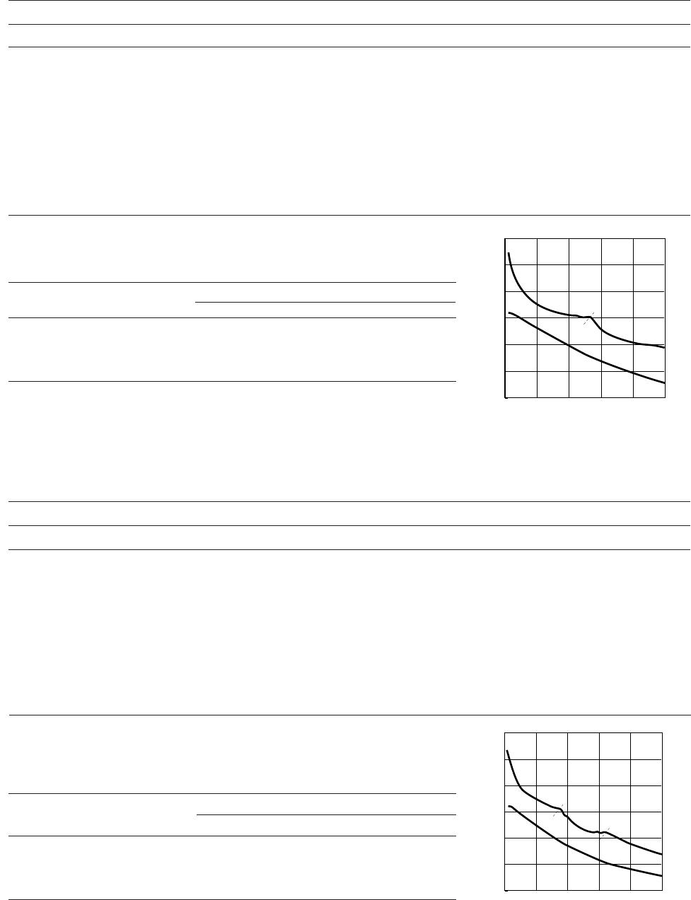
AT-32011 fig 19
GAIN (dB)
0
0
FREQUENCY (GHz)
2 3
30
1 5
10
4
20
MSG
MAG
S21
Figure 19. AT-32011 Gains vs. Frequency at V
CE
= 2.7 V,
I
C
= 2 mA.
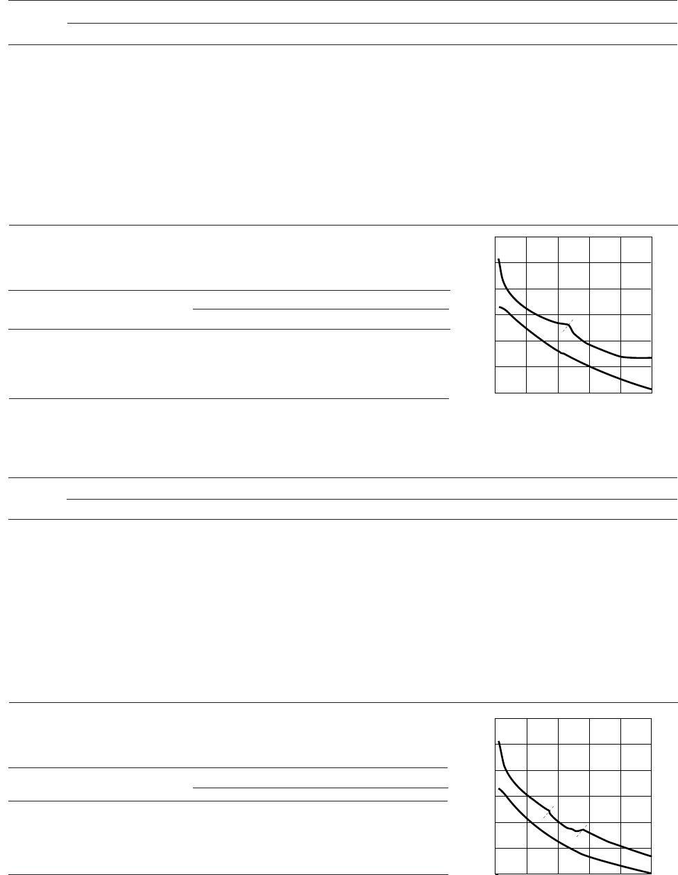
AT-32011 fig 20
GAIN (dB)
0
0
FREQUENCY (GHz)
2 3
30
1 5
10
4
20
MSG
MAG
S21
MSG
Figure 20. AT-32033 Gains vs. Frequency at V
CE
= 2.7 V,
I
C
= 2 mA.
AT-32033 Typical Scattering Parameters, Common Emitter, Zo = 50 Ω, V
CE
= 2.7 V, I
C
= 2 mA
Freq. S
11
S
21
S
12
S
22
GHz Mag Ang dB Mag Ang dB Mag Ang Mag Ang
0.1 0.93 -13 16.61 6.77 167 -34.89 0.018 82 0.99 -6
0.5 0.68 -56 14.29 5.18 127 -23.10 0.070 61 0.83 -22
0.9 0.44 -86 11.48 3.75 101 -20.35 0.096 55 0.71 -30
1.0 0.39 -93 10.88 3.50 96 -19.91 0.101 54 0.70 -31
1.5 0.23 -129 8.16 2.56 76 -17.99 0.126 55 0.64 -36
1.8 0.18 -156 6.89 2.21 66 -16.89 0.143 57 0.62 -39
2.0 0.16 -176 6.19 2.04 60 -16.14 0.156 57 0.61 -42
2.4 0.17 146 4.91 1.76 50 -14.70 0.184 58 0.60 -47
3.0 0.22 108 3.35 1.47 36 -12.51 0.237 57 0.58 -56
4.0 0.32 76 1.51 1.19 18 -9.19 0.347 51 0.55 -73
5.0 0.40 56 0.17 1.02 4 -6.54 0.471 40 0.51 -95
AT-32033 Typical Noise Parameters,
Common Emitter, Zo = 50 Ω, 2.7 V, I
C
= 2 mA
Freq. F
min
R
n
GHz dB Mag Ang –
0.5
[1]
0.57 0.77 15 0.36
0.9 0.78 0.63 49 0.28
1.8 1.25 0.32 136 0.10
2.4 1.57 0.40 -159 0.08
Note:
1. 0.5 GHz noise parameter values are extrapolated, not measured.
Γ
opt
AT-32011 Typical Noise Parameters,
Common Emitter, Zo = 50 Ω, 2.7 V, I
C
= 2 mA
Freq. F
min
R
n
GHz dB Mag Ang –
0.5
[1]
0.57 0.69 22 0.30
0.9 0.78 0.60 51 0.25
1.8 1.25 0.42 117 0.14
2.4 1.57 0.44 159 0.08
Note:
1. 0.5 GHz noise parameter values are extrapolated, not measured.
Γ
opt