DMOS Dual Full-Bridge PWM Motor Driver
With Overcurrent Protection
A4987
13
Allegro MicroSystems, LLC
115 Northeast Cutoff, Box 15036
Worcester, Massachusetts 01615-0036 (508) 853-5000
www.allegromicro.com
0
100.0
66.7
33.3
–33.3
–100.0
–66.7
0
100.0
66.7
33.3
–33.3
–100.0
–66.7
(%)
Phase 1
(%)
Phase 2
Figure 7. Step Sequence for Quarter-Step Increments
Step Sequencing Settings
Full 1/2 1/4
Phase 1
(%I
TripMax
)
I01 I11 PHASE
Phase 2
(%I
TripMax
)
I02 I12 PHASE
11 0 HHx 100LL1
2 33 L H 1 100 L L 1
1 2 3 100/66* L/H* L 1 100/66* L/H* L 1
4 100 L L 1 33 L H 1
3 5 100 L L 1 0 H H X
6 100 L L 1 33 L H 0
2 4 7 100/66* L/H* L 1 100/66* L/H* L 0
8 33 L H 1 100 L L 0
59 0 HHx 100LL0
10 33 L H 0 100 L L 0
3 6 11 100/66* L/H* L 0 100/66* L/H* L 0
12 100 L L 0 33 L H 0
7 13 100 L L 0 0 H H X
14 100 L L 0 33 L H 1
4 8 15 100/66* L/H* L 0 100/66* L/H* L 1
16 33 L H 0 100 L L 1
* Denotes modified step mode
DMOS Dual Full-Bridge PWM Motor Driver
With Overcurrent Protection
A4987
14
Allegro MicroSystems, LLC
115 Northeast Cutoff, Box 15036
Worcester, Massachusetts 01615-0036 (508) 853-5000
www.allegromicro.com
Terminal List Table
Name
Number
Description
ES LP
CP1 4 1 Charge pump capacitor terminal
CP2 5 2 Charge pump capacitor terminal
PH1 17 14 Logic input
PH2 2 23 Logic input
GND 3, 16 13, 24 Ground*
IN02 8 5 Logic input
IN12 9 6 Logic input
NC No connection
OUT1A 21 18 DMOS Full Bridge 1 Output A
OUT1B 18 15 DMOS Full Bridge 1 Output B
OUT2A 22 19 DMOS Full Bridge 2 Output A
OUT2B 1 22 DMOS Full Bridge 2 Output B
REF 15 12 G
m
reference voltage input
IN11 10 7 Logic input
ROSC 11 8 Timing set
SENSE1 20 17 Sense resistor terminal for Bridge 1
SENSE2 23 20 Sense resistor terminal for Bridge 2
¯
S
¯
¯
L
¯
¯
E
¯
¯
E
¯
¯
P
¯
12 9 Logic input
IN01 14 11 Logic input
VBB1 19 16 Load supply
VBB2 24 21 Load supply
VCP 6 3 Reservoir capacitor terminal
VDD 13 10 Logic supply
VREG 7 4 Regulator decoupling terminal
PAD Exposed pad for enhanced thermal dissipation*
*The GND pins must be tied together externally by connecting to the PAD ground plane under the device.
PAD
18
17
16
15
14
13
1
2
3
4
5
6
7
8
9
10
11
12
24
23
22
21
20
19
VBB2
SENSE2
OUT2A
OUT1A
SENSE1
VBB1
VREG
IN02
IN12
IN11
ROSC
SLEEP
OUT1B
PH1
GND
REF
IN01
VDD
OUT2B
PH2
GND
CP1
CP2
VCP
Pin-out Diagrams
ES Package LP Package
1
2
3
4
5
6
7
8
9
10
11
12
24
23
22
21
20
19
18
17
16
15
14
13
GND
PH2
OUT2B
VBB2
SENSE2
OUT2A
OUT1A
SENSE1
VBB1
OUT1B
PH1
GND
CP1
CP2
VCP
VREG
IN02
IN12
IN11
ROSC
SLEEP
VDD
IN01
REF
PAD
DMOS Dual Full-Bridge PWM Motor Driver
With Overcurrent Protection
A4987
15
Allegro MicroSystems, LLC
115 Northeast Cutoff, Box 15036
Worcester, Massachusetts 01615-0036 (508) 853-5000
www.allegromicro.com
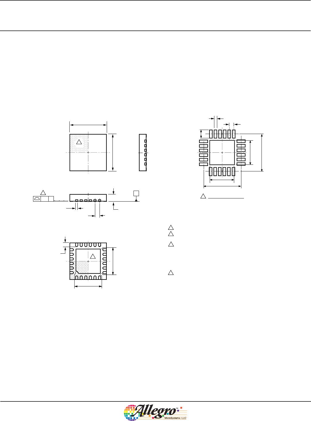
ES Package, 24-Pin QFN with Exposed Thermal Pad
0.95
C
SEATING
PLANE
C0.08
25X
24
24
2
1
1
2
24
2
1
A
A
Terminal #1 mark area
Coplanarity includes exposed thermal pad and terminals
B
Exposed thermal pad (reference only, terminal #1
identifier appearance at supplier discretion)
For Reference Only; not for tooling use (reference JEDEC MO-220WGGD)
Dimensions in millimeters
Exact case and lead configuration at supplier discretion within limits shown
C
D
D
C
Reference land pattern layout (reference IPC7351
QFN50P400X400X80-25W6M)
All pads a minimum of 0.20 mm from all adjacent pads; adjust as necessary
to meet application process requirements and PCB layout tolerances; when
mounting on a multilayer PCB, thermal vias at the exposed thermal pad land
can improve thermal dissipation (reference EIA/JEDEC Standard JESD51-5)
4.10
0.30
0.50
4.10
0.50 BSC
4.00 ±0.15
4.00 ±0.15
2.70
2.70
2.70
2.70
0.75 ±0.05
0.45 MAX
B
PCB Layout Reference View
0.25
+0.05
–0.07

APEK4987SLP-01-T-DK

Mfr. #:
Manufacturer:
Description:
BOARD EVAL MOTOR CONTROL A4987
Lifecycle:
New from this manufacturer.
Delivery:
DHL FedEx Ups TNT EMS
Payment:
T/T Paypal Visa MoneyGram Western Union

Products related to this Datasheet