DMOS Dual Full-Bridge PWM Motor Driver
With Overcurrent Protection
A4987
7
Allegro MicroSystems, LLC
115 Northeast Cutoff, Box 15036
Worcester, Massachusetts 01615-0036 (508) 853-5000
www.allegromicro.com
Charge Pump (CP1 and CP2). The charge pump is used to
generate a gate supply greater than that of VBB for driving the
source-side FET gates. A 0.1 μF ceramic capacitor, should be
connected between CP1 and CP2. In addition, a 0.1 μF ceramic
capacitor is required between VCP and VBB, to act as a reservoir
for operating the high-side FET gates.
Capacitor values should be Class 2 dielectric ±15% maximum,
or tolerance R, according to EIA (Electronic Industries Alliance)
specifications.
V
REG
(VREG). This internally-generated voltage is used to
operate the sink-side FET outputs. The nominal output voltage
of the VREG terminal is 7 V. The VREG pin must be decoupled
with a 0.22 μF ceramic capacitor to ground. V
REG
is internally
monitored. In the case of a fault condition, the FET outputs of the
A4987 are disabled.
Capacitor values should be Class 2 dielectric ±15% maximum,
or tolerance R, according to EIA (Electronic Industries Alliance)
specifications.
Shutdown. In the event of a fault, overtemperature (excess T
J
)
or an undervoltage (on VCP), the FET outputs of the A4987 are
disabled until the fault condition is removed. At power-on, the
UVLO (undervoltage lockout) circuit disables the FET outputs
and resets the translator to the Home state.
Sleep Mode (
¯
S
¯
¯
L
¯
¯
E
¯
¯
E
¯
¯
P
¯
). To minimize power consumption
when the motor is not in use, this input disables much of the
internal circuitry including the output FETs, current regulator, and
charge pump. A logic low on the S
¯
¯
L
¯
¯
E
¯
¯
E
¯
¯
P
¯
pin puts the A4987 into
Sleep mode. When emerging from Sleep mode, in order to allow
the charge pump to stabilize, provide a delay of 1 ms before issu-
ing a logic command.
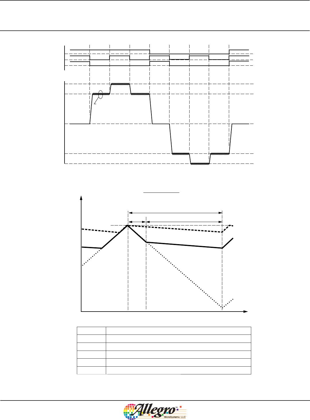
Mixed Decay Operation. The bridge operates in Mixed
Decay mode, as shown in figures 5 through 7. As the trip point
is reached, the A4987 initially goes into a fast decay mode for
31.25% of the off-time, t
OFF
. After that, it switches to Slow Decay
mode for the remainder of t
OFF
. A timing diagram for this feature
appears in figure 4.
Synchronous Rectification. When a PWM-off cycle is
triggered by an internal fixed-off time cycle, load current recir-
culates in Mixed Decay mode. This synchronous rectification
feature turns on the appropriate FETs during current decay, and
effectively shorts out the body diodes with the low FET R
DS(ON)
.
This reduces power dissipation significantly, and can eliminate
the need for external Schottky diodes in many applications. Syn-
chronous rectification turns off when the load current approaches
zero (0 A), preventing reversal of the load current.
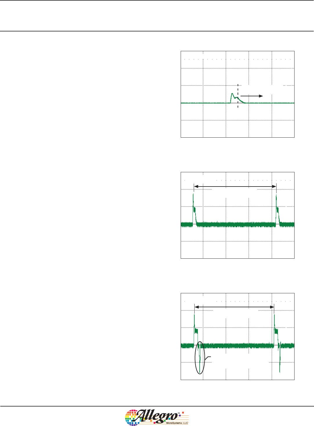
t
Fixed off-time
5 A / div.
t
5 A / div.
Figure 2. Shorted load (OUTxA OUTxB) in
Slow decay mode
Figure 3. Shorted load (OUTxA OUTxB) in Mixed decay mode
Fixed off-time
Fast decay portion
(direction change)
t
Fault latched
5 A / div.
Figure 1. Short-to-ground event
DMOS Dual Full-Bridge PWM Motor Driver
With Overcurrent Protection
A4987
8
Allegro MicroSystems, LLC
115 Northeast Cutoff, Box 15036
Worcester, Massachusetts 01615-0036 (508) 853-5000
www.allegromicro.com
Symbol Characteristic
t
off
Device fixed off-time
I
PEAK
Maximum output current
t
SD
Slow decay interval
t
FD
Fast decay interval
I
OUT
Device output current
Figure 4. Current Decay Modes Timing Chart
I
OUT
I
OUT
t
See Enlargement A
Enlargement A
t
SD
t
FD
t
off
Slow Decay
Mixed Decay
Fast Decay
I
PEAK
70.71
–70.71
0
100.00
–100.00
PHx
IN0x
IN1x
DMOS Dual Full-Bridge PWM Motor Driver
With Overcurrent Protection
A4987
9
Allegro MicroSystems, LLC
115 Northeast Cutoff, Box 15036
Worcester, Massachusetts 01615-0036 (508) 853-5000
www.allegromicro.com
Application Layout
Layout. The printed circuit board should use a heavy ground-
plane. For optimum electrical and thermal performance, the
A4987 must be soldered directly onto the board. On the under-
side of the A4987 package is an exposed pad, which provides a
path for enhanced thermal dissipation. The thermal pad should be
soldered directly to an exposed surface on the PCB. Thermal vias
are used to transfer heat to other layers of the PCB.
In order to minimize the effects of ground bounce and offset
issues, it is important to have a low impedance single-point
ground, known as a star ground, located very close to the device.
By making the connection between the pad and the ground plane
directly under the A4987, that area becomes an ideal location for
a star ground point. A low impedance ground will prevent ground
bounce during high current operation and ensure that the supply
voltage remains stable at the input terminal.
The two input capacitors should be placed in parallel, and as
close to the device supply pins as possible. The ceramic capaci-
tor (CIN1) should be closer to the pins than the bulk capacitor
(CIN2). This is necessary because the ceramic capacitor will be
responsible for delivering the high frequency current components.
The sense resistors, R
Sx
, should have a very low impedance
path to ground, because they must carry a large current while
supporting very accurate voltage measurements by the current
sense comparators. Long ground traces will cause additional
voltage drops, adversely affecting the ability of the comparators
to accurately measure the current in the windings. The SENSEx
pins have very short traces to the R
Sx
resistors and very thick,
low impedance traces directly to the star ground underneath the
device. If possible, there should be no other components on the
sense circuits.
PCB
Thermal Vias
Trace (2 oz.)
Signal (1 oz.)
Ground (1 oz.)
Thermal (2 oz.)
Solder
A4987
V
DD
V
BB
C2
ROSC
PAD
A4987
C6
C7
C3
C4
R4
R5
C1
OUT2B
OUT1A
OUT1BOUT2A
VBB2
SENSE2
OUT2A
OUT1A
SENSE1
VBB1
OUT2B
PH2
GND
CP1
CP2
VCP
OUT1B
PH1
GND
REF
IN01
VDD
VREG
IN02
IN12
IN11
ROSC
SLEEP
R4
U1
OUT2B
GND
R5
OUT2A
OUT1A
OUT1B
GND
GND
GND
C3
C4
C6
ROSC
C2
C7
C1
VBBVDD
CAPACITANCE
BULK
ES package configuration shown

APEK4987SLP-01-T-DK

Mfr. #:
Manufacturer:
Description:
BOARD EVAL MOTOR CONTROL A4987
Lifecycle:
New from this manufacturer.
Delivery:
DHL FedEx Ups TNT EMS
Payment:
T/T Paypal Visa MoneyGram Western Union

Products related to this Datasheet