Low Capacitance, Low Charge Injection,
±15 V/+12 V iCMOS Quad SPST Switches
Data Sheet
ADG1211/ADG1212/ADG1213
Rev. D Document Feedback
Information furnished by Analog Devices is believed to be accurate and reliable. However, no
responsibility is assumed by Analog Devices for its use, nor for any infringements of patents or other
rights of third parties that may result from its use. Specifications subject to change without notice. No
license is granted by implication or otherwise under any patent or patent rights of Analog Devices.
Trademarks and registered trademarks are the property of their respective owners.
One Technology Way, P.O. Box 9106, Norwood, MA 02062-9106, U.S.A.
Tel: 781.329.4700 ©20052016 Analog Devices, Inc. All rights reserved.
Technical Support www.analog.com
FEATURES
1 pF off capacitance
2.6 pF on capacitance
<1 pC charge injection
33 V supply range
120 Ω on resistance
Fully specified at ±15 V, +12 V
No V
L
supply required
3 V logic-compatible inputs
Rail-to-rail operation
16-lead TSSOP and 16-lead LFCSP
Typical power consumption: <0.03 µW
APPLICATIONS
Automatic test equipment
Data acquisition systems
Battery-powered systems
Sample-and-hold systems
Audio signal routing
Video signal routing
Communication systems
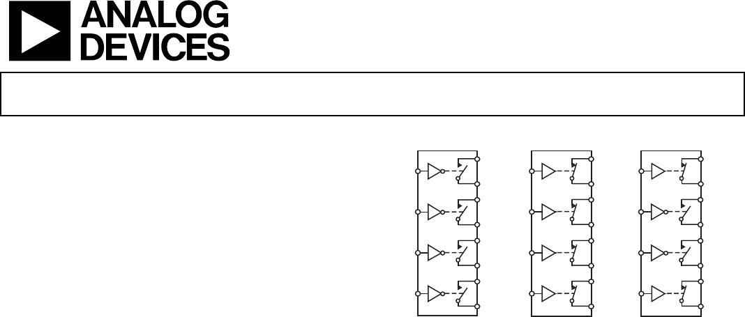
FUNCTIONAL BLOCK DIAGRAM
IN1
IN2
IN3
IN4
S1
D1
S2
D2
S3
D3
S4
D4
ADG1211
SWITCHES SHOWN FOR A LOGIC 1 INPUT
IN1
IN2
IN3
IN4
S1
D1
S2
D2
S3
D3
S4
D4
ADG1212
IN1
IN2
IN3
IN4
S1
D1
S2
D2
S3
D3
S4
D4
ADG1213
04778-001
Figure 1.
GENERAL DESCRIPTION
The ADG1211/ADG1212/ADG1213 are monolithic complemen-
tary metal-oxide semiconductor (CMOS) devices containing
four independently selectable switches designed on an iCMOS®
(industrial CMOS) process. iCMOS is a modular manufacturing
process combining high voltage CMOS and bipolar technologies.
It enables the development of a wide range of high performance
analog ICs capable of 33 V operation in a footprint that no previous
generation of high voltage devices has been able to achieve.
Unlike analog ICs using conventional CMOS processes, iCMOS
components can tolerate high supply voltages while providing
increased performance, dramatically lower power consumption,
and reduced package size.
The ultralow capacitance and charge injection of these switches
make them ideal solutions for data acquisition and sample-and-
hold applications, where low glitch and fast settling are required.
Fast switching speed coupled with high signal bandwidth make
the devices suitable for video signal switching.
iCMOS construction ensures ultralow power dissipation,
making the devices ideally suited for portable and battery-
powered instruments.
The ADG1211/ADG1212/ADG1213 contain four independent
single-pole/single-throw (SPST) switches. The ADG1211 and
ADG1212 differ only in that the digital control logic is inverted.
The ADG1211 switches are turned on with Logic 0 on the
appropriate control input, while Logic 1 is required for the
ADG1212. The ADG1213 has two switches with digital control
logic similar to that of the ADG1211; the logic is inverted on the
other two switches. The ADG1213 exhibits break-before-make
switching action for use in multiplexer applications.
Each switch conducts equally well in both directions when on
and has an input signal range that extends to the supplies. In the
off condition, signal levels up to the supplies are blocked.
PRODUCT HIGHLIGHTS
1. Ultralow capacitance.
2. <1 pC charge injection.
3. 3 V logic-compatible digital inputs: V
IH
= 2.0 V, V
IL
= 0.8 V.
4. No V
L
logic power supply required.
5. Ultralow power dissipation: <0.03 µW.
6. 16-lead TSSOP and 3 mm × 3 mm LFCSP packages.
ADG1211/ADG1212/ADG1213 Data Sheet
Rev. D | Page 2 of 16
TABLE OF CONTENTS
Features .............................................................................................. 1
Applications ....................................................................................... 1
Functional Block Diagram .............................................................. 1
General Description ......................................................................... 1
Product Highlights ........................................................................... 1
Revision History ............................................................................... 2
Specifications ..................................................................................... 3
Dual Supply ................................................................................... 3
Single Supply ................................................................................. 5
Absolute Maximum Ratings ............................................................6
ESD Caution...................................................................................6
Pin Configurations and Function Descriptions ............................7
Terminology .......................................................................................8
Typical Performance Characteristics ..............................................9
Test Circuits ..................................................................................... 12
Outline Dimensions ....................................................................... 14
Ordering Guide .......................................................................... 15
REVISION HISTORY
11/2016Rev. C to Rev. D
Change to VDD Parameter, Table 2 ............................................... 5
3/2016Rev. B to Rev. C
Changes to Figure 3 .......................................................................... 7
Updated Outline Dimensions ....................................................... 14
Changes to Ordering Guide .......................................................... 15
8/2012Rev. A to Rev. B
Changes to Table 1 ............................................................................ 3
Changes to Table 2 ............................................................................ 5
Change to Table 6 ............................................................................. 7
Updated Outline Dimensions ....................................................... 14
Changes to Ordering Guide .......................................................... 15
2/2009Rev. 0 to Rev. A
Changes to Power Requirements, I
DD
, Digital Inputs = 5 V
Parameter, Table 1 ............................................................................. 4
Changes to Power Requirements, I
DD
, Digital Inputs = 5 V
Parameter, Table 2 ............................................................................. 5
7/2005Revision 0: Initial Version
Data Sheet ADG1211/ADG1212/ADG1213
Rev. D | Page 3 of 16
SPECIFICATIONS
DUAL SUPPLY
V
DD
= 15 V ± 10%, V
SS
= −15 V ± 10%, GND = 0 V, unless otherwise noted.
Table 1.
Y Version
1
Parameter 25°C
−40°C to
+85°C
−40°C to
+125°C Unit Test Conditions/Comments
ANALOG SWITCH
Analog Signal Range V
DD
to V
SS
V
On Resistance (R
ON
) 120 typ V
S
= ±10 V, I
S
= −1 mA; see Figure 20
190 230 260 max V
DD
= +13.5 V, V
SS
= −13.5 V
On Resistance Match Between
Channels (∆R
ON
)
2.5 typ V
S
= ±10 V, I
S
= −1 mA
6 10 11 max
On Resistance Flatness (R
FL AT (ON)
) 20 typ V
S
= −5 V/0 V/+5 V; I
S
= −1 mA
57 72 79 max
LEAKAGE CURRENTS V
DD
= +16.5 V, V
SS
= −16.5 V
Source Off Leakage, I
S
(Off ) ±0.02 nA typ
V
S
= ±10 V, V
D
=
10 V; see Figure 21
±0.1 ±0.6 ±1 nA max
Drain Off Leakage, I
D
(Off ) ±0.02 nA typ
V
S
= ±10 V, V
D
=
10 V; see Figure 21
±0.1 ±0.6 ±1 nA max
Channel On Leakage, I
D
, I
S
(On) ±0.02 nA typ V
S
= V
D
= ±10 V; see Figure 22
±0.1 ±0.6 ±1 nA max
DIGITAL INPUTS
Input High Voltage, V
INH
2.0 V min
Input Low Voltage, V
INL
0.8 V max
Input Current, I
INL
or I
INH
0.005 µA typ V
IN
= V
INL
or V
INH
±0.1
µA max
Digital Input Capacitance, C
IN
2.5 pF typ
2
t
ON
110 ns typ R
L
= 300 Ω, C
L
= 35 pF
130 160 195 ns max V
S
= 10 V; see Figure 23
t
OFF
85 ns typ R
L
= 300 Ω, C
L
= 35 pF
115 130 150 ns max V
S
= 10 V; see Figure 23
Break-Before-Make Time Delay, t
D
25 ns typ R
L
= 300 Ω, C
L
= 35 pF
(ADG1213 Only) 10 ns min V
S1
= V
S2
= 10 V; see Figure 24
Charge Injection −0.3 pC typ V
S
= 0 V, R
S
= 0 Ω, C
L
= 1 nF; see Figure 25
Off Isolation 80 dB typ R
L
= 50 Ω, C
L
= 5 pF, f = 1 MHz; see Figure 26
Channel-to-Channel Crosstalk 90 dB typ R
L
= 50 , C
L
= 5 pF, f = 1 MHz; see Figure 27
Total Harmonic Distortion + Noise 0.15 % typ R
L
= 10 kΩ, 5 V rms, f = 20 Hz to 20 kHz
−3 dB Bandwidth 1000 MHz typ R
L
= 50 Ω, C
L
= 5 pF; see Figure 28
S
0.9
pF typ
V
S
= 0 V, f = 1 MHz
1.1 pF max V
S
= 0 V, f = 1 MHz
C
D
(Off ) 1 pF typ V
S
= 0 V, f = 1 MHz
1.2 pF max V
S
= 0 V, f = 1 MHz
C
D
, C
S
(On) 2.6 pF typ V
S
= 0 V, f = 1 MHz
3 pF max V
S
= 0 V, f = 1 MHz

ADG1212YRUZ

Mfr. #:
Manufacturer:
Analog Devices Inc.
Description:
Analog Switch ICs IC 120 Ohm 16.2V iCMOS Quad SPST
Lifecycle:
New from this manufacturer.
Delivery:
DHL FedEx Ups TNT EMS
Payment:
T/T Paypal Visa MoneyGram Western Union