NCP605, NCP606
http://onsemi.com
4
ELECTRICAL CHARACTERISTICS
V
in
= (V
out
+ 0.5 V) or 1.5 V, whichever is higher, C
in
= 1 mF, C
out
= 1 mF, for typical values T
A
= 25°C, for min/max values T
A
= 40°C to
85°C; unless otherwise noted. (Notes 9 and 10)
Parameter
Test Conditions Symbol Min Typ Max Unit
Output voltage (Adjustable Version) V
in
= 1.75 V to 6 V
I
out
= 1 mA to 500 mA
V
out
1.231
(1.5%)
1.250 1.269
(+1.5%)
V
Output voltage (Fixed Versions) 1.5 V
1.8 V
2.5 V
2.8 V
3.0 V
3.3 V
5.0 V
V
in
= (V
out
+ 0.5 V) to 6 V
I
out
= 1 mA to 500 mA
V
out
1.470
1.764
2.450
2.744
2.940
3.234
4.900
(2%)
1.5
1.8
2.5
2.8
3.0
3.3
5.0
1.530
1.836
2.550
2.856
3.060
3.366
5.100
(+2%)
V
Line regulation V
in
= (V
out
+ 0.5 V) to 6 V, I
out
= 1 mA Reg
line
4 10 mV
Load regulation I
out
= 1 mA to 500 mA Reg
load
10 30 mV
Dropout voltage (Adjustable Version)
(Note 9)
V
DO
= V
in
V
out
V
out
= 1.25 V
I
out
= 500 mA
V
DO
450 470
mV
Dropout voltage (Fixed Version)
1.5 V
1.8 V
2.5 V
2.8 V
3.0 V
3.3 V
5.0 V
V
DO
= V
in
(V
out
0.1 V)
I
out
= 500 mA
V
out
= 0 V to 90% V
out(nom)
V
DO
290
250
200
190
180
170
150
360
300
250
240
230
220
200
mV
Disable Current (NCP606 Only) (Note 10) V
EN
= 0 V I
DIS
0.1 1
mA
Ground Current I
out
= 1 mA to 500 mA I
GND
145 180
mA
Current Limit (Note 11) V
out
= V
out(nom)
10 % I
LIM
675 mA
Output Short Circuit Current V
out
= 0 V I
SC
700 1000 1350 mA
Enable Input Threshold Voltage
(NCP606 Only)
Voltage Increasing, Logic High
Voltage Decreasing, Logic Low
High
Low
V
th(EN)
0.9
0.4
V
Turnon Time (Note 11)
1.25 V
1.5 V
1.8 V
2.5 V
2.8 V
3.0 V
3.3 V
5.0 V
V
in
= 0 V to (V
out
+ 0.5 V) or 1.75 V,
whichever is higher
V
out
= 0 V to 90% of V
out(nom)
t
on
6
6
7
8
10
12
15
30
ms
Enable Time (NCP606 Only) (Note 11)
1.25 V
1.5 V
1.8 V
2.5 V
2.8 V
3.0 V
3.3 V
5.0 V
V
EN
= From 0 V to V
in
t
EN
12
12
13
16
18
19
20
30
ms
7. Refer to ABSOLUTE MAXIMUM RATINGS and APPLICATION INFORMATION for Safe Operating Area.
8. Performance guaranteed over the indicated operating temperature range by design and/or characterization tested at T
J
= T
A
= 25°C. Low
duty cycle pulse techniques are used during testing to maintain the junction temperature as close to ambient as possible.
9. Maximum dropout voltage is limited to minimum input voltage V
in
= 1.7 V recommended for guaranteed operation at maximum output
current.
10.Refer to application information section.
11. Values based on design and/or characterization.
NCP605, NCP606
http://onsemi.com
5
ELECTRICAL CHARACTERISTICS
V
in
= (V
out
+ 0.5 V) or 1.5 V, whichever is higher, C
in
= 1 mF, C
out
= 1 mF, for typical values T
A
= 25°C, for min/max values T
A
= 40°C to
85°C; unless otherwise noted. (Notes 9 and 10)
Parameter UnitMaxTypMinSymbolTest Conditions
Power Supply Ripple Rejection (Note 11) I
out
= 500 mA
V
out
= 1.25 V
V
in
V
out
= 1 V
f = 120 Hz, 0.5 V
PP
f = 1 kHz, 0.5 V
PP
f = 10 kHz, 0.5 V
PP
PSRR
62
55
40
dB
Output Noise Voltage (Note 11) f = 10 Hz to 100 kHz, V
out
= 1.25 V V
n
50
mV
rms
Thermal Shutdown Temperature (Note 11) T
SD
175 °C
Thermal Shutdown Hysteresis (Note 11) T
SH
10 °C
7. Refer to ABSOLUTE MAXIMUM RATINGS and APPLICATION INFORMATION for Safe Operating Area.
8. Performance guaranteed over the indicated operating temperature range by design and/or characterization tested at T
J
= T
A
= 25°C. Low
duty cycle pulse techniques are used during testing to maintain the junction temperature as close to ambient as possible.
9. Maximum dropout voltage is limited to minimum input voltage V
in
= 1.7 V recommended for guaranteed operation at maximum output
current.
10.Refer to application information section.
11. Values based on design and/or characterization.
NCP605, NCP606
http://onsemi.com
6
TYPICAL CHARACTERISTICS
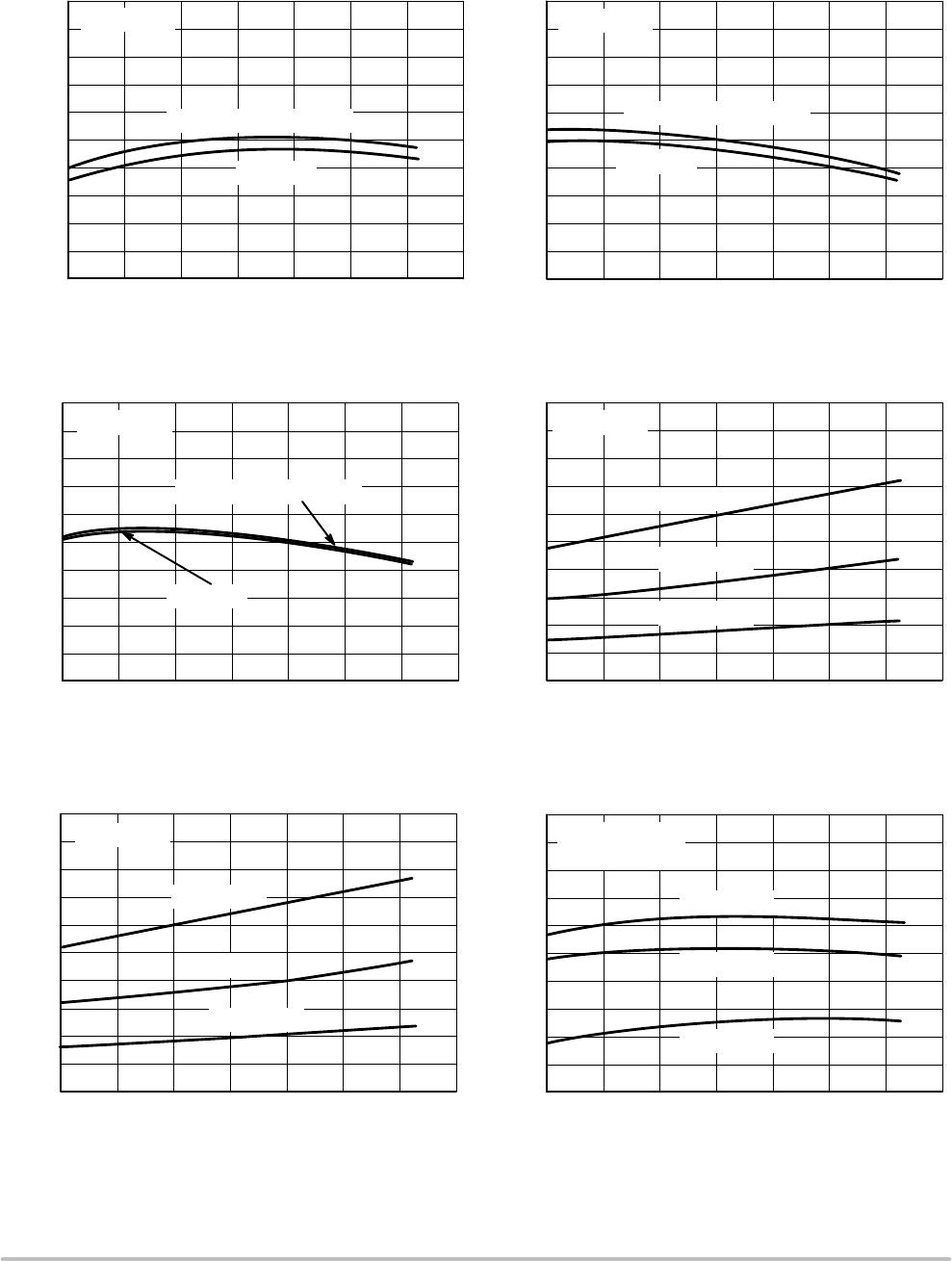
Figure 9. Output Voltage vs. Temperature
(V
out
= 1.25 V)
1.231
1.2348
1.2386
1.2424
1.2462
1.25
1.2538
1.2576
1.2614
1.2652
1.269
40 20 0 20 40 60 80 100
T
A
, AMBIENT TEMPERATURE (°C)
V
out
, OUTPUT VOLTAGE (V)
V
in
= V
out
+ 0.5 V = 1.75 V
V
in
= 6.0 V
V
out
= 1.25 V
Figure 10. Output Voltage vs. Temperature
(V
out
= 2.5 V)
2.45
2.46
2.47
2.48
2.49
2.5
2.51
2.52
2.53
2.54
2.55
40 20 0 20 40 60 80 100
T
A
, AMBIENT TEMPERATURE (°C)
V
out
, OUTPUT VOLTAGE (V)
V
in
= V
out
+ 0.5 V = 3.0 V
V
in
= 6.0 V
V
out
= 2.5 V
Figure 11. Output Voltage vs. Temperature
(V
out
= 5.0 V)
4.9
4.92
4.94
4.96
4.98
5
5.02
5.04
5.06
5.08
5.1
40 20 0 20 40 60 80 100
V
out
, OUTPUT VOLTAGE (V)
T
A
, AMBIENT TEMPERATURE (°C)
V
in
= 6.0 V
V
in
= V
out
+ 0.5 V = 5.5 V
Figure 12. Dropout Voltage vs. Temperature
(V
out
= 2.5 V)
0
30
60
90
120
150
180
210
240
270
300
40 20 0 20 40 60 80 100
V
DO
, DROPOUT VOLTAGE (mV)
T
A
, AMBIENT TEMPERATURE (°C)
I
out
= 500 mA
I
out
= 300 mA
I
out
= 150 mA
Figure 13. Dropout Voltage vs. Temperature
(V
out
= 5.0 V)
0
20
40
60
80
100
120
140
160
180
200
40 20 0 20 40 60 80 100
T
A
, AMBIENT TEMPERATURE (°C)
V
DO
, DROPOUT VOLTAGE (mV)
I
out
= 150 mA
I
out
= 300 mA
I
out
= 500 mA
Figure 14. Ground Current vs. Temperature
80
90
100
110
120
130
140
150
160
170
180
40 200 204060801
0
T
A
, AMBIENT TEMPERATURE (°C)
I
GND
, GROUND CURRENT (mA)
V
out
= 5.0 V
V
out
= 2.5 V
V
out
= 1.25 V
V
in
= V
out
+ 0.5 V
I
out
= 500 mA
V
out
= 5.0 V V
out
= 2.5 V
V
out
= 5.0 V

NCP605MN15T2G

Mfr. #:
Manufacturer:
ON Semiconductor
Description:
LDO Voltage Regulators 500mA ACMOS LDO
Lifecycle:
New from this manufacturer.
Delivery:
DHL FedEx Ups TNT EMS
Payment:
T/T Paypal Visa MoneyGram Western Union