Expand menu
Hello, Sign in
My Account
0
Cart
Home
Products
Sensors
Semiconductors
Passive Components
Connectors
Power
Electromechanical
Optoelectronics
Circuit Protection
Integrated Circuits - ICs
Main Products
Manufacturers
Blog
Services
About OMO
About Us
Contact Us
Check Stock
BAS28,235
P1-P3
P4-P6
P7-P9
P10-P12
P13-P13
BAS28
All informatio
n provided in thi
s document is su
bject to legal
disclaimers.
© NXP B.V
. 2010. All rights reserv
ed.
Product data sheet
Rev
. 3 — 22 July 2010
6 of 12
NXP Semiconductors
BAS28
High-speed double diode
8. T
est
information
8.1
Quality i
nformation
This product has been qualified in accordance
with the Automotive Electronics
Council
(AEC) standard
Q101 - S
tress test qualifica
t
ion for discrete semiconductors
, and is
suitable for use in auto
motive applications.
(1)
I
R
=1m
A
Fig 6.
Reverse recovery time test circuit and
waveforms
Fig 7.
Forward recovery voltage test circuit and waveforms
t
rr
(1)
+
I
F
t
output signal
t
r
t
p
t
10 %
90 %
V
R
input signal
V = V
R
+
I
F
×
R
S
R
S
= 50
Ω
I
F
D.U.T.
R
i
= 50
Ω
SAMPLING
OSCILLOSCOPE
mga881
t
r
t
t
p
10 %
90 %
I
input signal
R
S
= 50
Ω
I
R
i
= 50
Ω
OSCILLOSCOPE
1 k
Ω
450
Ω
D.U.T.
mga88
2
V
FR
t
output signal
V
BAS28
All informatio
n provided in thi
s document is su
bject to legal
disclaimers.
© NXP B.V
. 2010. All rights reserv
ed.
Product data sheet
Rev
. 3 — 22 July 2010
7 of 12
NXP Semiconductors
BAS28
High-speed double diode
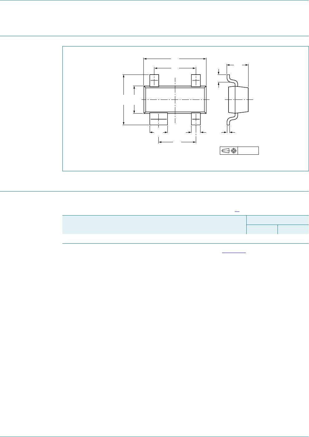
9. Package
outline
10. Packing
information
[1]
For further information and the avai
lability of packing methods, see
Section 14
.
Fig 8.
Package outline BAS28
(SOT143B)
04-11-16
Dimensions in mm
3.0
2.8
1.1
0.9
2.5
2.1
1.4
1.2
1.7
1.9
0.48
0.38
0.15
0.09
0.45
0.15
0.88
0.78
2
1
3
4
T
able 8.
Packing methods
The indicated -xxx are the last thre
e digits of the 12NC ordering code.
[1]
Ty
p
e
n
u
m
b
e
r
Package
Description
Packing quan
tity
3
000
10
000
BAS28
SOT143B
4 mm pitch, 8 m
m tape and reel
-215
-235
BAS28
All informatio
n provided in thi
s document is su
bject to legal
disclaimers.
© NXP B.V
. 2010. All rights reserv
ed.
Product data sheet
Rev
. 3 — 22 July 2010
8 of 12
NXP Semiconductors
BAS28
High-speed double diode
1
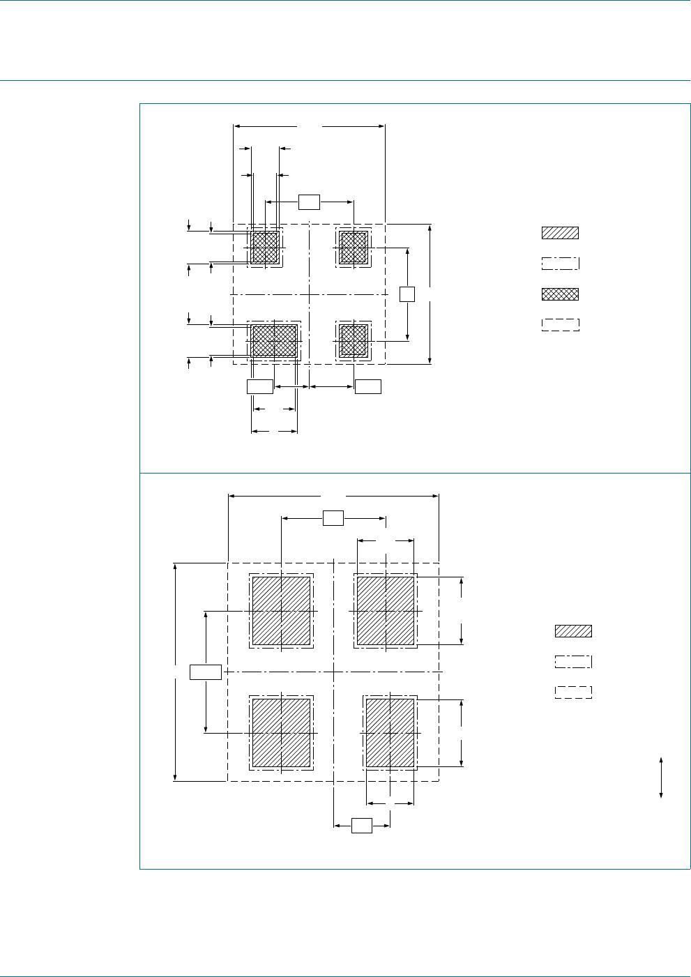
1. Soldering
Fig 9.
Reflow soldering footprint BAS28
(SOT143B)
Fig 10.
Wave soldering footprin
t BAS28 (SOT143
B)
solder lands
solder resist
occupied area
solder paste
sot143b_
fr
0.9
0.6
0.7
3.25
3
0.6
(3
×
)
0.6
(3
×
)
0.5
(3
×
)
0.7
(3
×
)
1
1.9
2
0.75
0.95
Dimensions in mm
solder lands
solder resist
occupied area
preferred transport direction during soldering
sot143b_
fw
4.6
4.45
1.2
(3
×
)
1.425
(3
×
)
1.425
1
1.2
2.2
2.575
Dimensions in mm
P1-P3
P4-P6
P7-P9
P10-P12
P13-P13
BAS28,235
Mfr. #:
Buy BAS28,235
Manufacturer:
Nexperia
Description:
Diodes - General Purpose, Power, Switching DIODE SW TAPE-11
Lifecycle:
New from this manufacturer.
Delivery:
DHL
FedEx
Ups
TNT
EMS
Payment:
T/T
Paypal
Visa
MoneyGram
Western
Union
Products related to this Datasheet
BAS28,215
BAS28,235