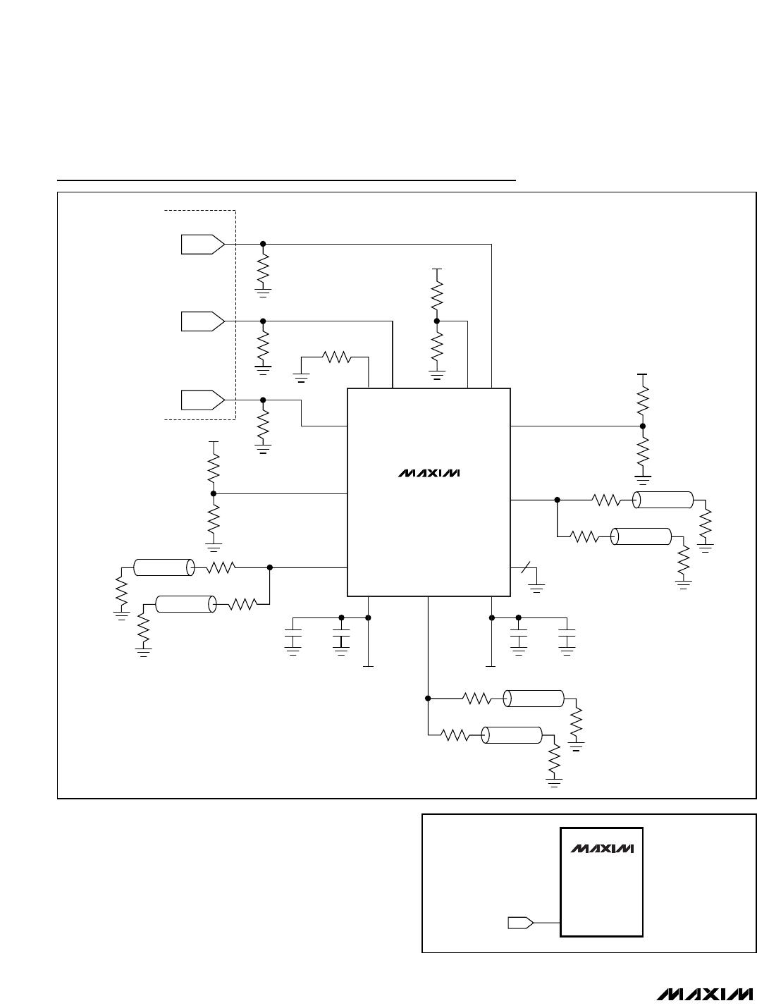
external resistors form a voltage-divider between V
CC
and GND. The values in the fourth column (V
HFB_
(V))
are calculated using the following equation:
V
HFB_
= V
CC
x R
HFB_-2
/ (R
HFB_-1
+ R
HFB_-2
)
where V
CC
= 5V.
Apply an external voltage to HFB_ in place of R
HFB_-1
and R
HFB_-2
as an alternative. See the Electrical
Characteristics section. Filter boost modes can also be
controlled from a microprocessor. See the Applications
Information section.
Filter Bypass
The MAX7438/MAX7439 offer selectable filter bypass-
ing that allows any of the video inputs to be filtered or
unfiltered. Select the filter bypass mode for a given
channel by setting the corresponding values for
R
HFB_-1
and R
HFB_-2
according to Table 1.
Output Buffer
The output buffer is able to drive two standard 150Ω
video loads with a 2V
P-P
signal. The MAX7438 output
buffer has a preset gain of 2V/V, and the MAX7439 out-
put buffer has a gain of 3V/V. The MAX7439 is ideal for
a DAC output whose voltage range is between 0.67V
and 1V. Set the DAC output to 0.67V to achieve a 2V/V
signal on OUT_.
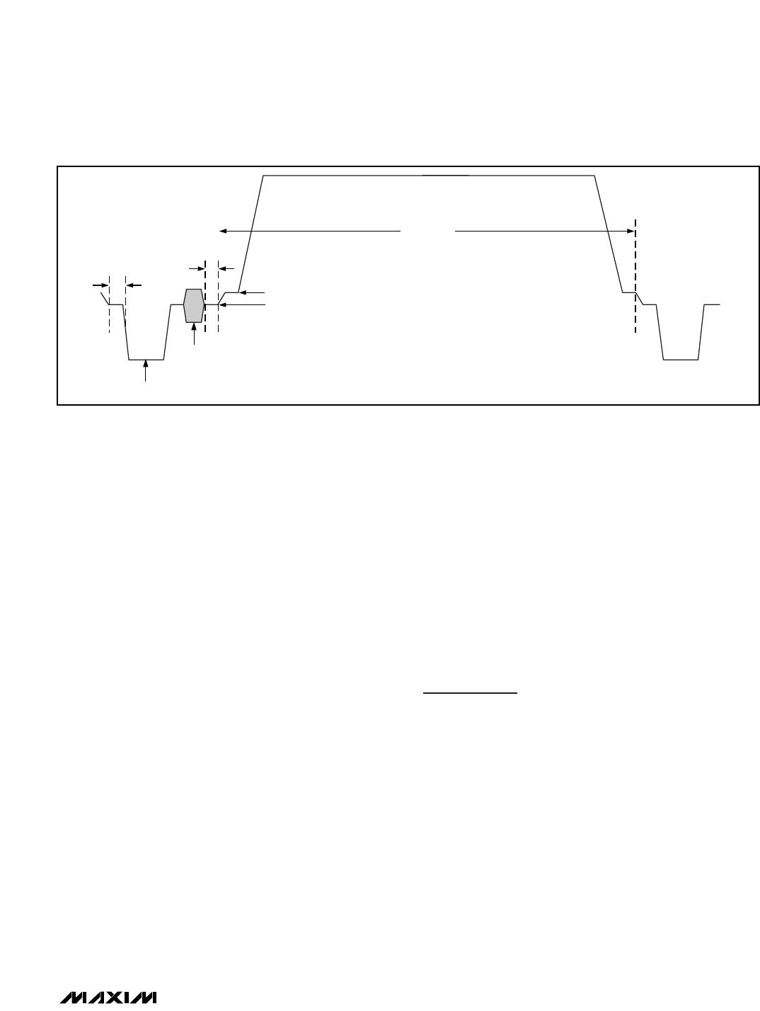
Back-Porch Clamp
The MAX7438/MAX7439 feature a back-porch clamp to
set the output blanking level. This clamp shifts the DC
level of the video signal so that the back-porch level is
close to ground (see Figure 1). The devices sense the
voltage during back porch and feed back into a control
system that provides the appropriate DC-level shift in
the filter channel to clamp the output to ground. The
back-porch clamp to ground eliminates the need for
large output-coupling capacitors that can introduce
unwanted line-time distortion (tilt), cost, and board
space. This feedback network and the on-chip capaci-
tors introduce a finite settling time (50 lines max) after
power-up or any dramatic shift in input voltage (see the
Electrical Characteristics section).
Channel 1 requires a video signal with sync information
(CVBS, Y, or G), since the other two channels are
clamped from channel 1. In the absence of a sync on
channel 1, the circuit forces all outputs actively and
continuously to ground.
Applications Information
Power-Supply Bypassing and Layout
The MAX7438/MAX7439 operate from dual ±5V sup-
plies. Bypass V
CC
and V
SS
to GND with 0.1µF capaci-
tors in parallel with 1µF capacitors. Place the 0.1µF
capacitors as close to the power inputs as possible.
Since EXT is a sensitive input, place R
EXT
close to the
device to avoid signals coupling into EXT. Do not route
any input, output, or dynamic signal near this pin and
the accompanying trace.
Note: The exposed paddle is electrically connected to
VSS.
Do not connect the exposed paddle to ground. Refer to
the MAX7438 EV kit for layout examples, as well as a
proven PC board layout example.
MAX7438/MAX7439
Triple-Channel Video Reconstruction Filters with
Back-Porch Clamp to GND
_______________________________________________________________________________________ 7