© Semiconductor Components Industries, LLC, 2009
March, 2009 − Rev. 4
1 Publication Order Number:
NCS2563/D
NCS2563
3-Channel Video Amp with
High Definition
Reconstruction Filters
Description
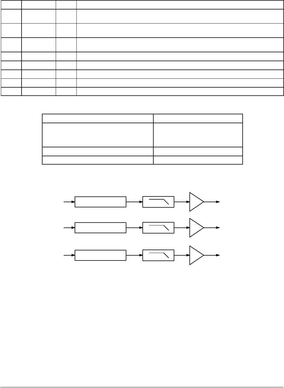
NCS2563 is a 3−Channel high speed video amplifier with 6th order
Butterworth High Definition (HD) reconstruction filters and 6 dB
gain.
All three channels can accommodate all Component and RGB video
signals. All channels can accept DC or AC coupled signals. If
AC coupled, the internal clamps are employed. The outputs can drive
both AC and DC coupled 150 W loads.
It is designed to be compatible with most Digital−to−Analog
Converters (DAC) embedded in most video processors.
Features
• Three 6th Order High Definition 30 MHz Filter
• Internally Fixed Gain = 6 dB
• Transparent Input Clamping for Each Channel
• DC or AC Coupled Inputs
• DC or AC Coupled Outputs
• Integrated Level Shifter
• Operating Voltage +5 V
• Available in SOIC−8 Package
• These are Pb−Free Devices
Applications
• Digital Set−Top Box
• DVD and Video Players
• HDTV
• Video−On−Demand (VOD)
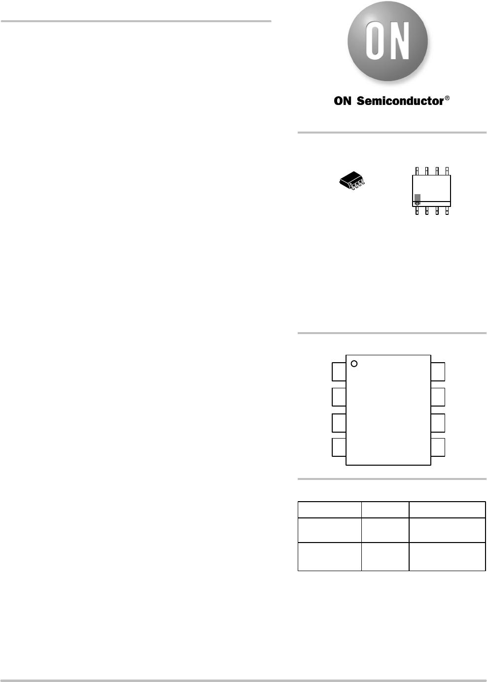
SOIC−8
D SUFFIX
CASE 751
MARKING DIAGRAM*
http://onsemi.com
N2563
ALYWG
G
1
8
A = Assembly Location
L = Wafer Lot
Y = Year
W = Work Week
G = Pb−Free Package
(Note: Microdot may be in either location)
Device Package Shipping
†
ORDERING INFORMATION
NCS2563DG SOIC−8
(Pb−Free)
98 Units / Rail
PINOUT
2
3
4
8
7
6
5
OUT1
OUT2
OUT3
IN1
IN2
IN3
GNDV
CC
NCS2563
SOIC−8
1
NCS2563DR2G SOIC−8
(Pb−Free)
2500 / Tape & Reel
†For information on tape and reel specifications,
including part orientation and tape sizes, please
refer to our Tape and Reel Packaging Specifications
Brochure, BRD8011/D.
1
8