NCS2563
http://onsemi.com
4
DC ELECTRICAL CHARACTERISTICS (V
CC
= +5.0 V, T
A
= 25°C, 0.1 mF AC coupled inputs, R
source
= 37.5 W, 220 mF AC
coupled outputs into 150 W load, referenced to 400 kHz, unless otherwise specified)
Symbol
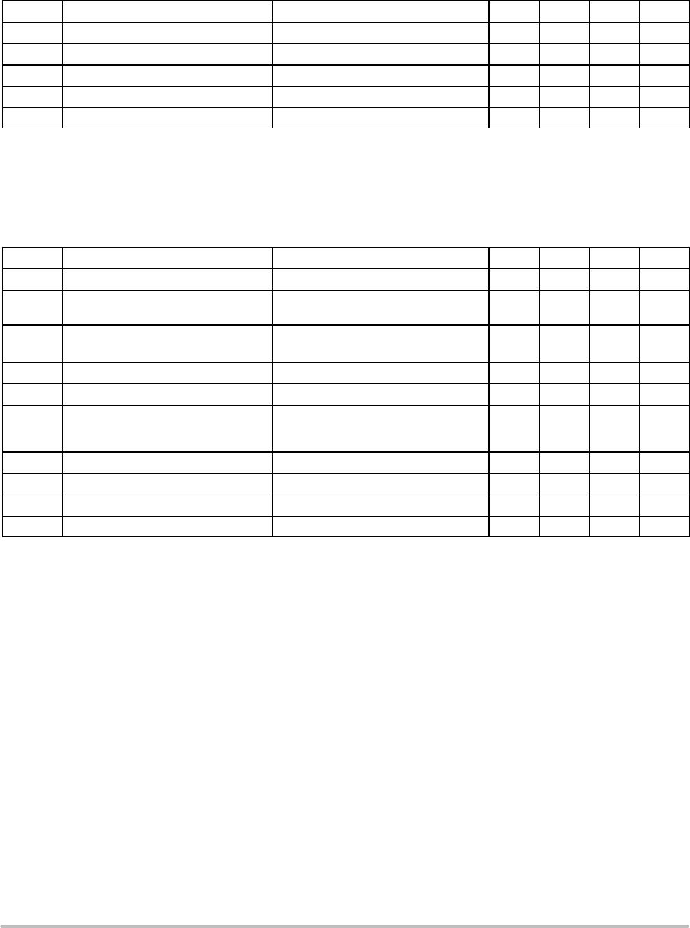
Characteristics Conditions Min Typ Max Unit
V
CC
Operating Voltage Range 4.75 5 5.25 V
I
CC
Power Supply Current 22 33 mA
V
IN
Input Common Mode Voltage Range GND 1.4 V
V
OH
Output High Voltage 2.8 V
V
OL
Output Low Voltage 280 mV
NOTE: Device will meet the specifications after thermal equilibrium has been established when mounted in a test socket or printed circuit
board with maintained transverse airflow greater than 500 lfpm. Electrical parameters are guaranteed only over the declared
operating temperature range. Functional operation of the device exceeding these conditions is not implied. Device specification limit
values are applied individually under normal operating conditions and not valid simultaneously.
AC ELECTRICAL CHARACTERISTICS (V
CC
= +5.0 V, T
A
= 25°C, 0.1 mF AC coupled inputs, R
source
= 37.5 W,220 mF AC
coupled outputs into 150 W load, referenced to 400 kHz, unless otherwise specified)
Symbol Characteristics Conditions Min Typ Max Unit
A
VOL
Voltage Gain (Note 5) V
IN
= 1 V 5.8 6.0 6.2 dB
BW Bandwidth of Low Pass Filter −1 dB
−3 dB
23 30
33
MHz
A
R
Attenuation (Stopband Reject) f = 44.25 MHz
f = 74.25 MHz 28
14.5
36
dG Differential Gain
A
V
= +2, R
L
= 150 W
0.2 %
dP Differential Phase
A
V
= +2, R
L
= 150 W
0.1 °
THD Total Harmonic Distortion V
OUT
= 1.4 V
PP
, f = 10 MHz
V
OUT
= 1.4 V
PP
, f = 15 MHz
V
OUT
= 1.4 V
PP
, f = 22 MHz
0.2
0.4
1.2
%
x
talk
Channel−to−Channel Crosstalk V
IN
= 1.4 V
PP
, f = 1 MHz 60 dB
SNR Signal to Noise Ratio* (Note 6) 100% White Signal, 100 kHz to 30 MHz 65 dB
t
PD
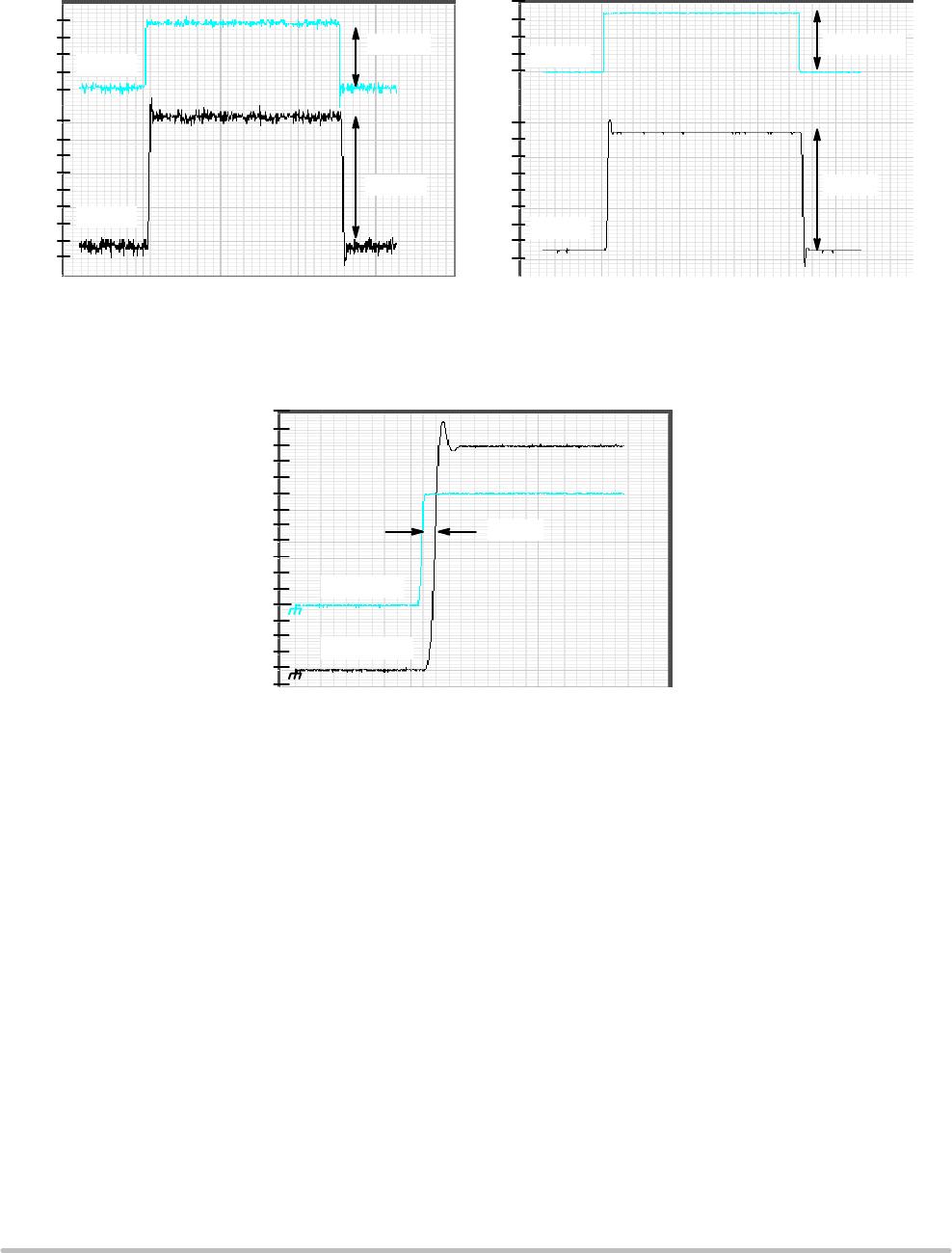
Propagation Delay Input to Output 20 ns
DTg
Group Delay Variation* 100 kHz to 30 MHz 6 ns
NOTE: Device will meet the specifications after thermal equilibrium has been established when mounted in a test socket or printed circuit
board with maintained transverse airflow greater than 500 lfpm. Electrical parameters are guaranteed only over the declared
operating temperature range. Functional operation of the device exceeding these conditions is not implied. Device specification limit
values are applied individually under normal operating conditions and not valid simultaneously.
*Guaranteed by design
5. 100% of tested IC fit to the bandwidth tolerance.
6. SNR = 20 x log (714 mV/RMS noise)


