LT3032 Series
16
3032ff
For more information www.linear.com/LT3032
The LT3032 is a dual 150mA positive and negative low noise
low dropout linear regulator with micropower quiescent
current and shutdown. It supplies ±150mA at a dropout
of 300mV. Output voltage noise can be lowered on the
positive side to 20µV
RMS
and to 30µV
RMS
on the negative
side over the 10Hz to 100kHz bandwidth with the addition
of 0.01µF reference bypass capacitors. Additionally, the
reference bypass capacitors improve transient response,
lowering the settling time for transient load conditions.
Quiescent current is 25µA for the positive side and –30µA
for the negative side (45µA each for the LT3032-12/
LT3032-15), typically dropping to less than 3µA total in
shutdown. In addition to the low quiescent current, the
LT3032 incorporates several protection features which
make it ideal for use in battery-powered systems. If the
load is common mode between the two outputs, it does
not matter which output starts first; either output can be
pulled to the opposing side of ground and the regulator
will still start and operate.
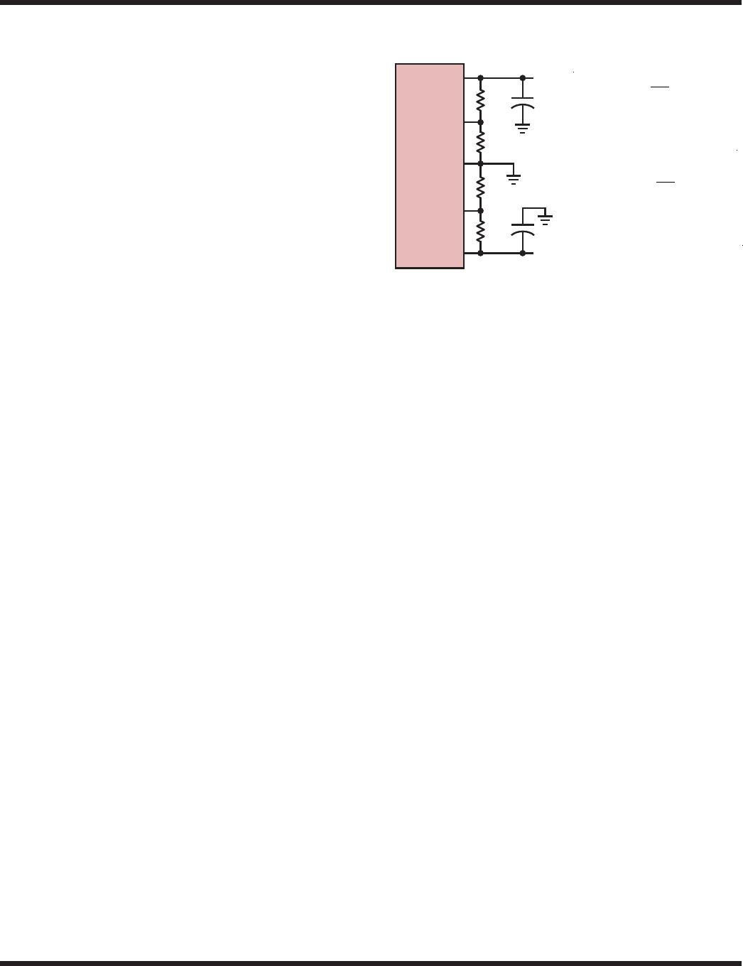
Setting Output Voltage
The adjustable LT3032 has output voltage ranges of 1.22V
to 20V for the positive side and –1.22V to –20V for the
negative side. The output voltages
are set by the ratio of
two external resistor dividers as shown in Figure 1. The
LT3032 servos the outputs to maintain the voltages at the
ADJP and ADJN pins to 1.22V and –1.22V, respectively.
The current in the bottom resistor of each divider (R1P
or R1N) is equal to 1.22V/R1 and the current in the top
resistor (R2P or R2N) is equal to the current in the bottom
resistor plus the respective ADJP/ADJN pin bias current.
The bias current for ADJP and ADJN is 30nA at 25°C,
flowing into the pin for ADJP and flowing out of the pin
for ADJN. The output voltages can then be calculated us
-
ing the
formulas shown in Figure 1. The value of R1P or
R1N
should be less than 250k to minimize errors in the
resultant output voltage caused by the ADJP/ADJN pin
bias current. Note that in shutdown the respective output
is turned off and the divider current will be zero. Curves
of ADJP Pin Voltage, ADJN Pin Voltage, ADJP Pin Bias
Current, and ADJN Pin Bias Current (all vs Temperature)
appear in the Typical Performance Characteristics.
The LT3032 is tested and specified
with the ADJP/ADJN
pin tied to the respective OUTP/OUTN pin and a ±5µA DC
load (unless otherwise specified) for an output voltage
of ±1.22V. Specifications for output voltages greater than
this will be proportional to ±1.22V; (V
OUT
/±1.22V). For
example, load regulation for an output current change
of 1mA to 150mA is –2mV typical at V
OUTN
= –1.22V. At
V
OUTN
= –12V, load regulation is:
(–12V/–1.22V)•(–2mV) = –19.6mV
Bypass Capacitors and Low Noise Performance
The LT3032 provides reasonable noise performance
without reference bypass capacitors from OUTP/OUTN
to the corresponding BYPP/BYPN pin. Using the LT3032
with the addition of reference bypass capacitors lowers
output voltage noise. Good quality low leakage capacitors
are recommended. These capacitors bypass the internal
references for the positive and negative sides of the LT3032,
providing low frequency noise poles. The noise poles
provided by the bypass capacitors decrease the output
voltage noise to as low as 20µV
RMS
for the positive side
and 30µV
RMS
for the negative side with the use of 0.01µF
bypass capacitors.
The BYPP pin and BYPN pin are high impedance nodes
and leakage into or out of these pins affects the reference
voltage. The BYPP pin operates
at approximately 74
mV at
Figure 1. Setting Output Voltages
APPLICATIONS INFORMATION
LT3032
OUTP
V
OUTP
V
OUTN
R2P
R1P
R1N
R2N
ADJP
GND
ADJN
OUTN
+
+
V
OUTP
=1.22V 1+
R2P
R1P
+ I
ADJP
( )
R2P
( )
V
ADJP
=1.22V
I
ADJP
= 30nA at 25°C
OUTPUT RANGE= 1.22V TO 20V
V
OUTN
= –1.22V 1+
R2N
R1N
+ I
ADJN
( )
R2N
( )
V
ADJN
= –1.22V
I
ADJN
= –30nA at 25°C
OUTPUT RANGE= –1.22V TO – 20V

