LT3032 Series
24
3032ff
For more information www.linear.com/LT3032
LINEAR TECHNOLOGY CORPORATION 2010
LT 0417 REV F • PRINTED IN USA
www.linear.com/LT3032
RELATED PARTS
PART NUMBER DESCRIPTION COMMENTS
LT1175 800mA Negative Low Dropout
Micropower Regulator
V
IN
: –4.5V to -20V, I
Q
= 45μA, 0.5V Dropout Voltage, S8, DD-Pak, TO-220 and SOT-223
Packages
LT1761 100mA, Low Noise LDO 300mV Dropout Voltage, Low Noise: 20µV
RMS
, V
IN
= 1.8V to 20V, ThinSOT package
LT1762 150mA, Low Noise LDO 300mV Dropout Voltage, Low Noise: 20µV
RMS
, V
IN
= 1.8V to 20V, MS8 package
LTC1844 150mA, Very Low Dropout LDO 80mV Dropout Voltage, Low Noise <30µV
RMS
, V
IN
= 1.6V to 6.5V, Stable with 1µF Output
Capacitors, ThinSOT Package
LT1962 300mA, Low Noise LDO 270mV Dropout Voltage, Low Noise: 20µV
RMS
, V
IN
= 1.8V to 20V, MS8 Package
LT1964 200mA, Low Noise, Negative LDO 340mV Dropout Voltage, Low Noise 30µV
RMS
, V
IN
= –1.8V to –20V, ThinSOT and
DFN Packages
LT3023 Dual
100mA, Low Noise, Micropower LDO V
IN
: 1.8V to 20V, V
OUT(MIN)
= 1.22V, VDO = 0.30V, I
Q
= 40μA, ISD < 1μA; DFN and
MS10E Packages
LT3024 Dual 100mA/500mA, Low Noise,
Micropower LDO
V
IN
: 1.8V to 20V, V
OUT(MIN)
= 1.22V, VDO = 0.30V, I
Q
= 60μA, ISD < 1μA; DFN and
TSSOP-16E Packages
LT3027 Dual 100mA, Low Noise, Micropower
LDO with Independent Inputs
V
IN
: 1.8V to 20V, V
OUT(MIN)
= 1.22V, VDO = 0.30V, I
Q
= 50μA, ISD < 1μA; DFN and
MS10E Packages
LT3028 Dual 100mA/500mA, Low Noise,
Micropower LDO with Independent Inputs
V
IN
: 1.8V to 20V, V
OUT(MIN)
= 1.22V, VDO = 0.32V, I
Q
= 60μA, ISD < 1μA; DFN and
TSSOP-16E Packages
LT3029 Dual 500mA/500mA, Low Dropout, Low
Noise, Micropower Linear Regulator
Low Noise: 20μV
RMS
(10Hz to 100kHz), Low Quiescent Current: 55μA per Channel Wide
Input Voltage Range: 1.8V to 20V (Common or Independent Input Supply) Adjustable
Output: 1.215V Reference, Very Low Quiescent Current in Shutdown: <1μA per Channel
Stable with 3.3μF Minimum Output Capacitor, Thermally Enhanced 16-Lead MSOP and
16-Lead (4mm × 3mm) DFN Packages
LT3082 200mA, Parallelable, Single Resistor, Low
Dropout Linear Regulator
Wide Input Voltage Range: 1.2V to 40V Low Value Input/Output Capacitors Required:
0.22μF, Single Resistor Sets Output Voltage Initial Set Pin Current Accuracy: 1%, Low
Output Noise: 40μV
RMS
(10Hz to 100kHz) Reverse-Battery Protection, Reverse-Current
Protection 8-Lead SOT-23, 3-Lead SOT-223 and 8-Lead 3mm × 3mm DFN Packages
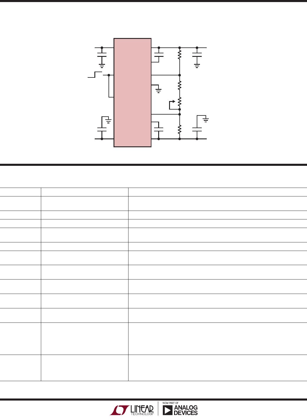
LT3032
INP
10µF
10µF
536k
536k
95.3k
250k
OUTP
5.5V TO
20V
–5.5V TO
–20V
OUTNINN
ADJP
BYPP
BYPN
ADJN
GND
SHDNP
SHDNN
0.01µF
0.01µF
5V TO 15V
AT 150mA
–5V TO –15V
AT –150mA
ON
±5V to ±15V Tracking Supply
TYPICAL APPLICATION