LTC2801/LTC2802/
LTC2803/LTC2804
2
2801234fe
abSolute MaxiMuM ratinGS
(Note 1)
Input Supplies
V
CC
...........................................................–0.3V to 7V
V
L
.........................................................–0.3V to 6.7V
Generated Supplies
V
DD
.................................................V
CC
–0.3V to 7.5V
V
EE
........................................................ 0.3V to –7.5V
V
DD
– V
EE
..............................................................14V
SW .................................................. –0.3V to V
DD
+ 0.3V
CAP .................................................. +0.3V to V
EE
– 0.3V
TIN, T1IN, T2IN, MODE ................................–0.3V to 7V
PS, ON/OFF .....................................–0.3V to (V
L
+ 0.3V)
RIN, R1IN, R2IN ..........................................–25V to 25V
TOUT, T1OUT, T2OUT.................................. –15V to 15V
ROUT, R1OUT, R2OUT ....................–0.3V to (V
L
+ 0.3V)
Operating Temperature
LT
C280XC ................................................0°C to 70°C
LT
C280XI .............................................–40°C to 85°C
Storage Temperature Range ..................–65°C to 125°C
Lead Temperature (Soldering, 10 sec)
GN Package ...................................................... 300°C
LTC2801, LTC2802
1-Driver/1-Receiver
LTC2803, LTC2804
2-Driver/2-Receiver
LTC2803-1, LTC2804-1
2-Driver/2-Receiver
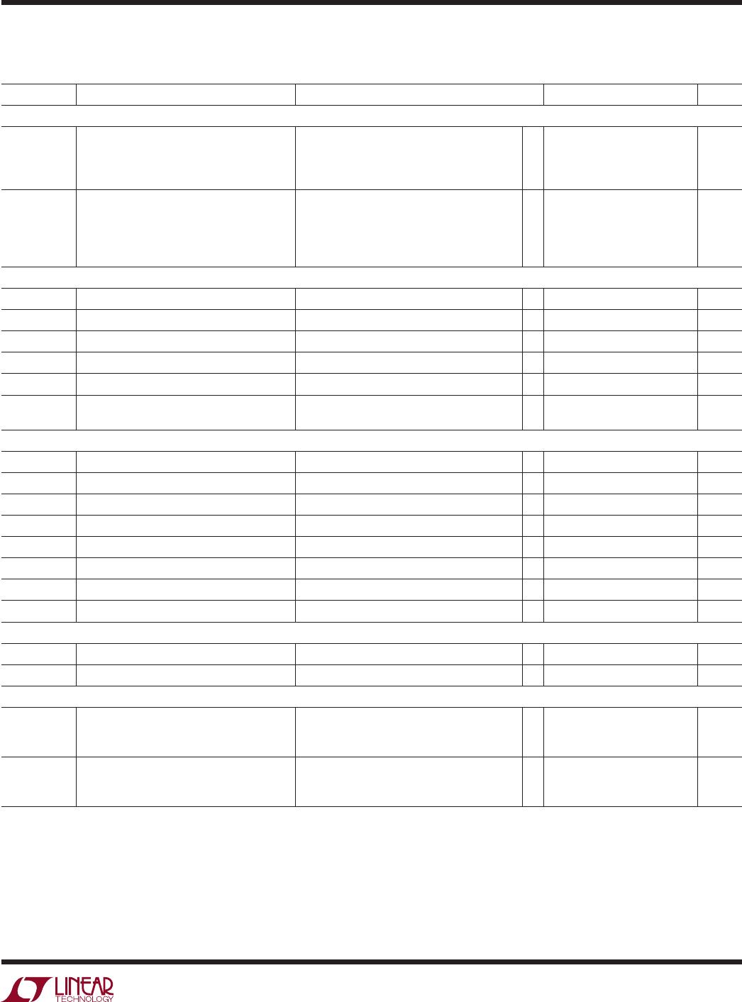
12
11
10
9
8
7
13
1
2
3
4
5
6
ROUT
TIN
V
L
MODE
PS
CAP
RIN
TOUT
V
CC
V
DD
SW
GND
TOP VIEW
DE PACKAGE
12-LEAD (4mm s 3mm) PLASTIC DFN
V
EE
T
JMAX
= 125°C, θ
JA
= 43°C/W, θ
JC
= 4.3°C/W (4 Layer)
EXPOSED PAD (PIN 13) IS V
EE
, MUST BE SOLDERED TO PCB
16
15
14
13
12
11
10
9
17
1
2
3
4
5
6
7
8
R1OUT
R2OUT
T1IN
T2IN
V
L
MODE
PS
CAP
R1IN
R2IN
T1OUT
T2OUT
V
CC
V
DD
SW
GND
TOP VIEW
DHC PACKAGE
16-LEAD (5mm s 3mm) PLASTIC DFN
V
EE
T
JMAX
= 125°C, θ
JA
= 44°C/W, θ
JC
= 4.3°C/W (4 Layer)
EXPOSED PAD (PIN 17) IS V
EE
, MUST BE SOLDERED TO PCB
GN PACKAGE
16-LEAD (NARROW 0.150) PLASTIC SSOP
1
2
3
4
5
6
7
8
TOP VIEW
16
15
14
13
12
11
10
9
R1OUT
R2OUT
T1IN
T2IN
V
L
ON/OFF
CAP
V
EE
R1IN
R2IN
T1OUT
T2OUT
V
CC
V
DD
SW
GND
T
JMAX
= 125°C, θ
JA
= 110°C/W, θ
JC
= 40°C/W (4 Layer)
Pin conFiGuration
LEAD FREE FINISH TAPE AND REEL PART MARKING* PACKAGE DESCRIPTION TEMPERATURE RANGE
LTC2801CDE#PBF LTC2801CDE#TRPBF 2801
12-Lead (4mm × 3mm) Plastic DFN
0°C to 70°C
LTC2801IDE#PBF LTC2801IDE#TRPBF 2801
12-Lead (4mm × 3mm) Plastic DFN
–40°C to 85°C
LTC2802CDE#PBF LTC2802CDE#TRPBF 2802
12-Lead (4mm × 3mm) Plastic DFN
0°C to 70°C
LTC2802IDE#PBF LTC2802IDE#TRPBF 2802
12-Lead (4mm × 3mm) Plastic DFN
–40°C to 85°C
LTC2803CDHC#PBF LTC2803CDHC#TRPBF 2803
16-Lead (5mm × 3mm) Plastic DFN
0°C to 70°C
LTC2803IDHC#PBF LTC2803IDHC#TRPBF 2803
16-Lead (5mm × 3mm) Plastic DFN
–40°C to 85°C
LTC2804CDHC#PBF LTC2804CDHC#TRPBF 2804
16-Lead (5mm × 3mm) Plastic DFN
0°C to 70°C
LTC2804IDHC#PBF LTC2804IDHC#TRPBF 2804
16-Lead (5mm × 3mm) Plastic DFN
–40°C to 85°C
LTC2803CGN-1#PBF LTC2803CGN-1#TRPBF 28031 16-Lead (Narrow 0.150) Plastic SSOP 0°C to 70°C
LTC2803IGN-1#PBF LTC2803IGN-1#TRPBF 2803I1 16-Lead (Narrow 0.150) Plastic SSOP –40°C to 85°C
LTC2804CGN-1#PBF LTC2804CGN-1#TRPBF 28041 16-Lead (Narrow 0.150) Plastic SSOP 0°C to 70°C
LTC2804IGN-1#PBF LTC2804IGN-1#TRPBF 2804I1 16-Lead (Narrow 0.150) Plastic SSOP –40°C to 85°C
Consult LTC Marketing for parts specified with wider operating temperature ranges. *The temperature grade is identified by a label on the shipping container.
Consult LTC Marketing for information on non-standard lead based finish parts.
For more information on lead free part marking, go to: http://www.linear.com/leadfree/
For more information on tape and reel specifications, go to: http://www.linear.com/tapeandreel/
order inForMation