LTC2801/LTC2802/
LTC2803/LTC2804
10
2801234fe
BOOST
REGULATOR
V
EE
V
DD
C3
1µF
C2
1µF
CAP
SW
C1
220nF
L1
10µH
V
CC
C4
1µF
C5
220nF
*OMIT IF V
L
IS CONNECTED TO V
CC
*
V
L
1.8V TO 5.5V
1.8V TO 5.5V
2801 F06
aPPlicationS inForMation
Overview
The LTC2801 family of RS-232 transceivers operates on
a V
CC
supply of 1.8V to 5.5V, utilizing a switching regula-
tor to generate the necessary higher voltage rails for the
drivers. The transceivers interface with logic operating
on any supply from 1.8V to 5.5V, independent of the V
CC
voltage. Depending on the device, one or two control pins
are available to invoke Shutdown, Receiver Active and
Driver Disable features.
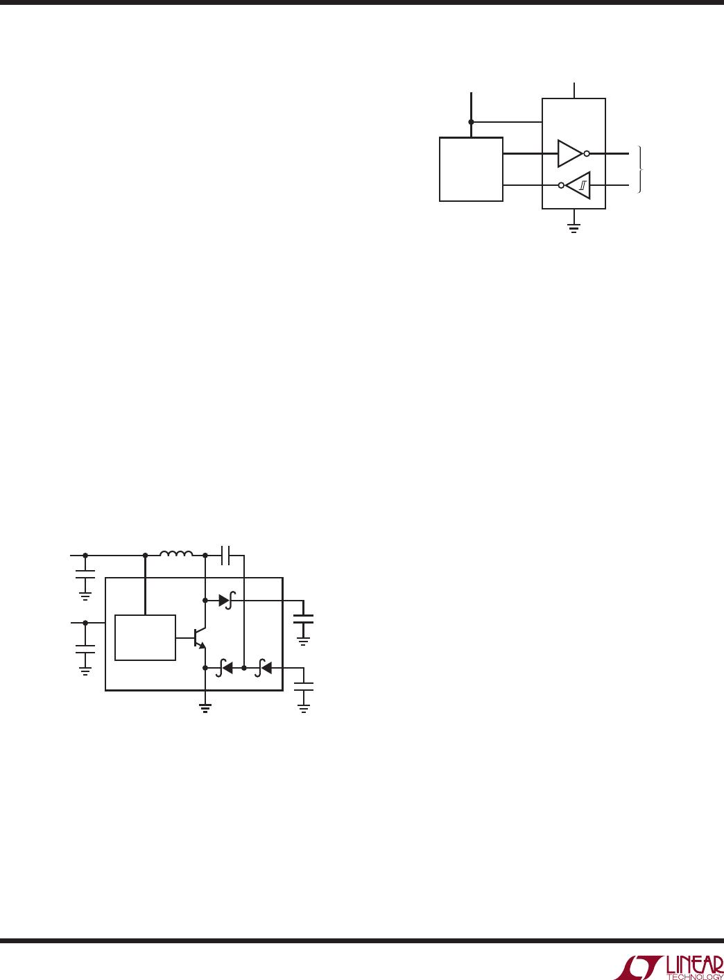
DC-DC Converter
The on-chip DC-DC converter operates from the V
CC
input, generating a 7V V
DD
supply and a charge pumped
6.3V V
EE
supply, as shown in Figure 6. V
DD
and V
EE
power the output stage of the drivers and are regulated
to levels that guarantee greater than ±5V output swing.
The DC-DC converter requires a 10µH inductor (L1) and
a bypass capacitor (C4) of at least 1µF. The recommended
size for the charge pump capacitor (C1) is 220nF and for
the storage capacitors (C2 and C3) is 1µF. Larger storage
capacitors up to 4.7µF may be used if C1 is kept at 20% to
50% their size and C4 is also scaled. Locate C1-C4 close
to their associated pins.
Power-Saving Modes
When the DC-DC converter and drivers are turned off (PS
and MODE or ON/OFF = logic low), V
CC
supply current is
reduced to 1µA. Tables 1 and 2 summarize the modes for
each device.
In Shutdown mode, V
L
supply current is reduced to 1µA,
and both receiver and driver outputs assume a high im-
pedance state.
In Receivers Active mode, the quiescent V
L
supply current
is reduced to 15µA and the driver outputs assume a high
impedance state. The receivers operate at a reduced rate
(typically 100 kbps) with hysteresis turned off.
Half-Duplex Operation
When the DC-DC converter is kept on (PS = logic high),
MODE serves as a low-latency driver enable for half-duplex
operation. Each driver is enabled and disabled in less than
2µs, while each receiver remains continuously active. This
mode of operation is illustrated in Figures 15-17.
Battery Operation
To maximize battery life, connect V
CC
(and L1) directly to
the unregulated battery voltage and V
L
to the regulated
supply, as shown in Figure 22. This configuration typically
minimizes conversion loss while providing compatibility
with system logic levels.
Inductor Selection
A 10µH inductor with a saturation current (I
SAT
) rating
of at least 200mA and low DCR (copper wire resistance)
is recommended. Some small inductors meeting these
requirements are listed in Table 3.
Figure 6. DC/DC Converter and Recommended Bypassing
V
L
Logic Supply
A separate logic supply pin V
L
allows the LTC2801 family to
interface with any logic signal from 1.8V to 5.5V, as shown
in Figure 7. Simply connect the desired logic supply to
V
L
. There is no interdependency between V
CC
and V
L
; they
may simultaneously operate at any voltage from 1.8V to
5.5V and sequence in any order. If V
L
is powered separately
from V
CC
, bypass V
L
with a 220nF capacitor (C5).
Figure 7. V
CC
and V
L
Are Independent
ANY VOLTAGE FROM
1.8V TO 5.5V
ANY VOLTAGE FROM
1.8V TO 5.5V
V
L
V
CC
EXTERNAL
DEVICE
RS-232
2801 F07
11
2801234fe
LTC2801/LTC2802/
LTC2803/LTC2804
Table 3. Recommended Inductors
PART
NUMBER
I
SAT
(mA)
MAX DCR
(Ω)
SIZE
(mm)
MANUFACTURER
LQH2MCN100K02L 225 1.2
2 × 1.6 × 0.95
Murata
www.murata.com
LBC2016T100K 245 0.85
2 × 1.6 × 1.6
Taiyo Yuden
www.t-yuden.com
FSLB2520-100K 220 1.1
2.5 × 2 × 1.6
Toko
www.tokoam.com
Capacitor Selection
The small size of ceramic capacitors makes them ideal for
the LTC2801 family. X5R and X7R (preferred) types are
recommended because their ESR is low and they retain their
capacitance over relatively wide voltage and temperature
ranges. Use a voltage rating of at least 10V.
Table 4. Recommended Ceramic Capacitor Manufacturers
MANUFACTURER URL
Murata www.murata.com
TDK www.tdk.com
Taiyo Yuden www.t-yuden.com
AVX www.avxcorp.com
Kemet www.kemet.com
Inrush Current and Supply Overshoot Precaution
In certain applications, such as battery-operated and
wall-adapter devices, fast supply slew rates are generated
when power is connected. If V
CC
s voltage is greater than
4.5V and its rise time is faster than 10µs, the pins V
DD
and SW can exceed their ABS MAX values during start-
up. When supply voltage is applied to V
CC
, the voltage
difference between V
CC
and V
DD
generates inrush current
V
L
V
L
V
CC
V
CC
GND
GND
GND
GND
GND
GND
GND
GND
GND
GND
C1
C1
C5
C5
C3
C3TOP VIEW
= VIA
TOP VIEW
= VIA
C4
C4
C2
C2
L1
L1
2801 F09
SW CAP
V
DD
GND
SCALE R1 WITH C1, C2, 1/C4
C1
220nF
L1
10µH
4.5V TO 5.5V
V
CC
R1
1/8W
C4
1µF
C2
1µF
INRUSH
CURRENT
2801 F08
aPPlicationS inForMation
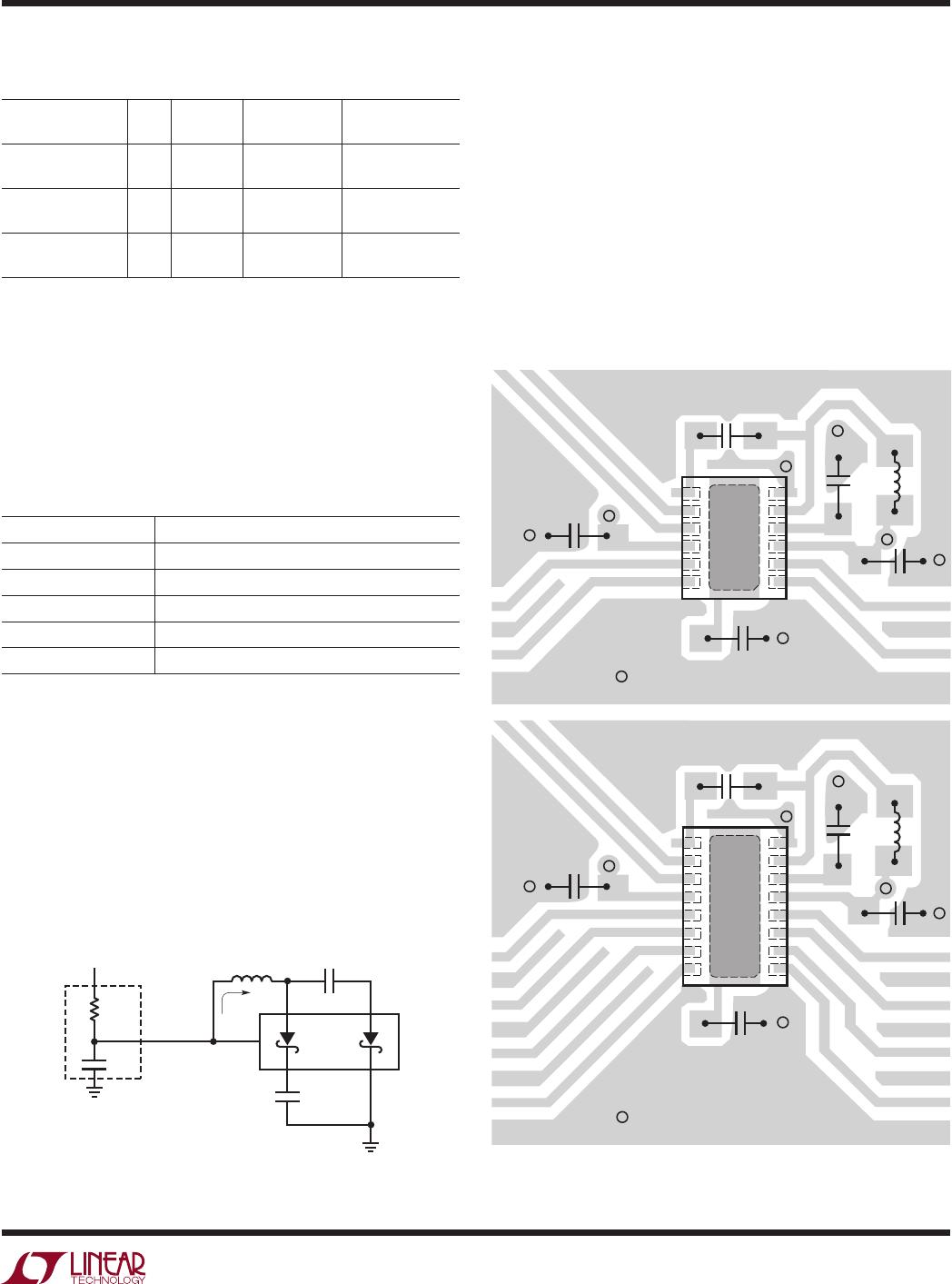
flowing through inductor L1 and capacitors C1, C2. The
peak inrush current must not exceed 2A. To avoid this
condition, add a resistor as shown in Figure 8. This
precaution is not relevant for supply voltages below 4.5V
or rise times longer than 10µs.
Board Layout
The board layout should minimize the length and area of
the SW and CAP traces. Suggested compact layouts for
the LTC2801 family are shown in Figure 9 (a) and (b).
Figure 9. Recommended Board Layouts for (a) Single and
(b) Dual Transceiver Parts
Figure 8. Supply Overshoot Protection for Input
Supplies of 4.5V or Higher
LTC2801/LTC2802/
LTC2803/LTC2804
12
2801234fe
2801 F17
LTC2803
R T
1.8V TO 5.5V
V
CC
V
L
PS
MODE
5
12
10
11
13
15
14
16
T2OUT
R2IN
T1OUT
R1IN
T2IN
R2OUT
T1IN
R1OUT
4
2
3
1
8
GND
3.3k
3.3k
2801 F16
LTC2802
R T
V
CC
V
L
PS
MODE
3
10
8
9
11
12
TOUT
RIN
TIN
ROUT
2
1
6
GND
3.3k
1.8V TO 5.5V
2801 F15
LTC2802
R T
V
CC
V
L
PS
MODE
3
10
8
9
11
12
TOUT
RIN
TIN
ROUT
2
1
6
GND
1.8V TO 5.5V
2801 F14
LTC2804-1
OFF ON
1.8V TO 5.5V
V
CC
V
L
ON/OFF
5
12
11
13
14
15
16
T2OUT
T1OUT
R2IN
R1IN
T2IN
T1IN
R2OUT
R1OUT
4
3
2
1
8
GND
2801 F13
LTC2802
V
CC
V
L
PS
MODE
3
10
8
9
11
12
TOUT
RIN
TIN
ROUT
2
1
6
GND
5V
µP
3V
2801 F12
LTC2801
V
CC
V
L
PS
MODE
3
10
8
9
11
12
TOUT
RIN
TIN
ROUT
2
1
6
GND
1.8V
µP
5V
2801 F11
LTC2804
V
CC
V
L
PS
MODE
5
12
10
11
13
14
15
16
T2OUT
T1OUT
R2IN
R1IN
T2IN
T1IN
R2OUT
R1OUT
4
3
2
1
RTS
TD
CTS
RD
V
BATT
RTS
TD
CTS
RD
8
GND
PERIPHERAL
CELL PHONE
1.8V TO 5.5V
tyPical aPPlicationS
2801 F10
LTC2803
RA ON
1.8V TO 5.5V
V
CC
V
L
MODE
PS
5
12
11
10
13
14
15
16
T2OUT
T1OUT
R2IN
R1IN
T2IN
T1IN
R2OUT
R1OUT
4
3
2
1
8
GND
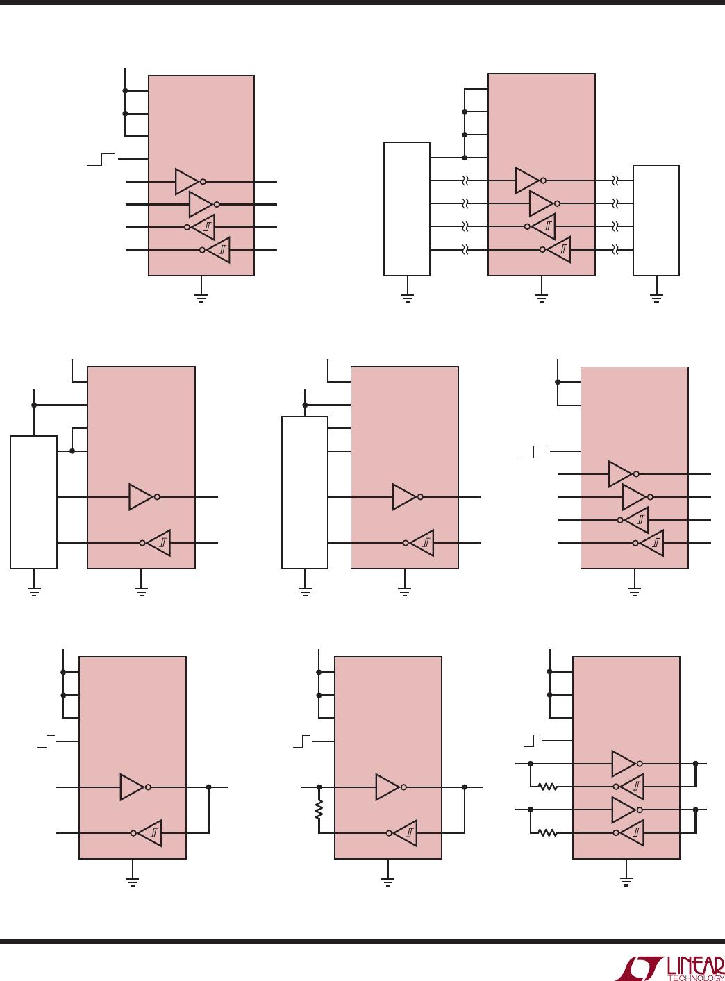
Figure 16. Half-Duplex on Single LineFigure 15. Half-Duplex on Single Line,
Separate ROUT, TIN
Figure 14. Power-Saving Shutdown ModeFigure 13. 5V Microprocessor InterfaceFigure 12. 1.8V Microprocessor Interface
Figure 11. Cellphone Peripheral InterfaceFigure 10. Power-Saving Receivers-Active Mode
Figure 17. Half-Duplex Dual Transceiver

LTC2803CDHC#TRPBF

Mfr. #:
Manufacturer:
Analog Devices Inc.
Description:
RS-232 Interface IC 1.8V-5V 2D+2R 250kbps RS232 Transceiver w/ Driver Disable
Lifecycle:
New from this manufacturer.
Delivery:
DHL FedEx Ups TNT EMS
Payment:
T/T Paypal Visa MoneyGram Western Union