LT3080
4
3080fc
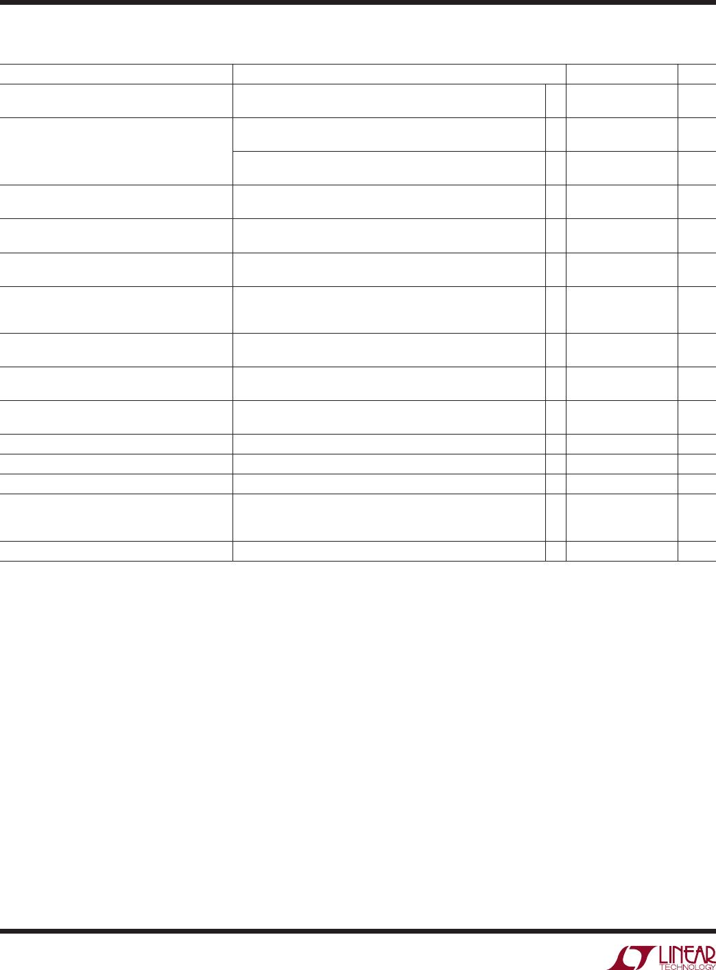
PARAMETER CONDITIONS MIN TYP MAX UNITS
SET Pin Current I
SET
V
IN
= 1V, V
CONTROL
= 2.0V, I
LOAD
= 1mA, T
J
= 25°C
V
IN
≥ 1V, V
CONTROL
≥ 2.0V, 1mA ≤ I
LOAD
≤ 1.1A (Note 9)
l
9.90
9.80
10
10
10.10
10.20
µA
µA
Output Offset Voltage (V
OUT
– V
SET
)
V
IN
= 1V, V
CONTROL
= 2V, I
OUT
= 1mA
V
OS
DFN and MSOP Package
l
–2
–3.5
2
3.5
mV
mV
SOT-223, DD-Pak and T0-220 Package
l
–5
–6
5
6
mV
mV
Load Regulation
ΔI
SET
ΔV
OS
ΔI
LOAD
=
1mA to 1.1A
ΔI
LOAD
=
1mA to 1.1A (Note 8)
l
–0.1
0.6
1.3
nA
mV
Line Regulation (Note 9)
DFN and MSOP Package
ΔI
SET
ΔV
OS
V
IN
= 1V to 25V, V
CONTROL
= 2V to 25V, I
LOAD
= 1mA
V
IN
= 1V to 25V, V
CONTROL
= 2V to 25V, I
LOAD
= 1mA
l
0.1
0.003
0.5 nA/V
mV/V
Line Regulation (Note 9)
SOT-223, DD-Pak and T0-220 Package
ΔI
SET
ΔV
OS
V
IN
= 1V to 26V, V
CONTROL
= 2V to 26V, I
LOAD
= 1mA
V
IN
= 1V to 26V, V
CONTROL
= 2V to 26V, I
LOAD
= 1mA
l
0.1
0.003
0.5 nA/V
mV/V
Minimum Load Current (Notes 3, 9) V
IN
= V
CONTROL
= 10V
V
IN
= V
CONTROL
= 25V (DFN and MSOP Package)
V
IN
= V
CONTROL
= 26V (SOT-223, DD-Pak and T0-220 Package)
l
l
l
300 500
1
1
µA
mA
mA
V
CONTROL
Dropout Voltage (Note 4) I
LOAD
= 100mA
I
LOAD
= 1.1A
l
1.2
1.35
1.6
V
V
V
IN
Dropout Voltage (Note 4) I
LOAD
= 100mA
I
LOAD
= 1.1A
l
l
100
350
200
500
mV
mV
V
CONTROL
Pin Current I
LOAD
= 100mA
I
LOAD
= 1.1A
l
l
4
17
6
30
mA
mA
Current Limit V
IN
= 5V, V
CONTROL
= 5V, V
SET
= 0V, V
OUT
= –0.1V
l
1.1 1.4 A
Error Amplifier RMS Output Noise (Note 6) I
LOAD
= 1.1A, 10Hz ≤ f ≤ 100kHz, C
OUT
= 10µF, C
SET
= 0.1µF 40 µV
RMS
Reference Current RMS Output Noise (Note 6) 10Hz ≤ f ≤ 100kHz 1 nA
RMS
Ripple Rejection f = 120Hz, V
RIPPLE
= 0.5V
P-P
, I
LOAD
= 0.2A, C
SET
= 0.1µF, C
OUT
= 2.2µF
f = 10kHz
f = 1MHz
75
55
20
dB
dB
dB
Thermal Regulation, I
SET
10ms Pulse 0.003 %/W
Note 1: Stresses beyond those listed under Absolute Maximum Ratings
may cause permanent damage to the device. Exposure to any Absolute
Maximum Rating condition for extended periods may affect device
reliability and lifetime.
Note 2: Unless otherwise specified, all voltages are with respect to V
OUT
.
The LT3080 is tested and specified under pulse load conditions such that
T
J
≅ T
A
. The LT3080E is tested at T
A
= 25°C. Performance of the LT3080E
over the full –40°C and 125°C operating temperature range is assured by
design, characterization, and correlation with statistical process controls.
The LT3080I is guaranteed over the full –40°C to 125°C operating junction
temperature range.
Note 3: Minimum load current is equivalent to the quiescent current of
the part. Since all quiescent and drive current is delivered to the output
of the part, the minimum load current is the minimum current required to
maintain regulation.
Note 4: For the LT3080, dropout is caused by either minimum control
voltage (V
CONTROL
) or minimum input voltage (V
IN
). Both parameters are
specified with respect to the output voltage. The specifications represent the
minimum input-to-output differential voltage required to maintain regulation.
Note 5: The V
CONTROL
pin current is the drive current required for the
output transistor. This current will track output current with roughly a 1:60
ratio. The minimum value is equal to the quiescent current of the device.
Note 6: Output noise is lowered by adding a small capacitor across the
voltage setting resistor. Adding this capacitor bypasses the voltage setting
resistor shot noise and reference current noise; output noise is then equal
to error amplifier noise (see Applications Information section).
Note 7: SET pin is clamped to the output with diodes. These diodes only
carry current under transient overloads.
Note 8: Load regulation is Kelvin sensed at the package.
Note 9: Current limit may decrease to zero at input-to-output differential
voltages (V
IN
–V
OUT
) greater than 25V (DFN and MSOP package) or 26V
(SOT-223, DD-Pak and T0-220 Package). Operation at voltages for both IN
and V
CONTROL
is allowed up to a maximum of 36V as long as the difference
between input and output voltage is below the specified differential
(V
IN
–V
OUT
) voltage. Line and load regulation specifications are not
applicable when the device is in current limit.
Note 10: This IC includes overtemperature protection that is intended
to protect the device during momentary overload conditions. Junction
temperature will exceed the maximum operating junction temperature when
overtemperature protection is active. Continuous operation above the specified
maximum operating junction temperature may impair device reliability.
Note 11: The SOT-223 package connects the IN and V
CONTROL
pins
together internally. Therefore, test conditions for this pin follow the
V
CONTROL
conditions listed in the Electrical Characteristics Table.
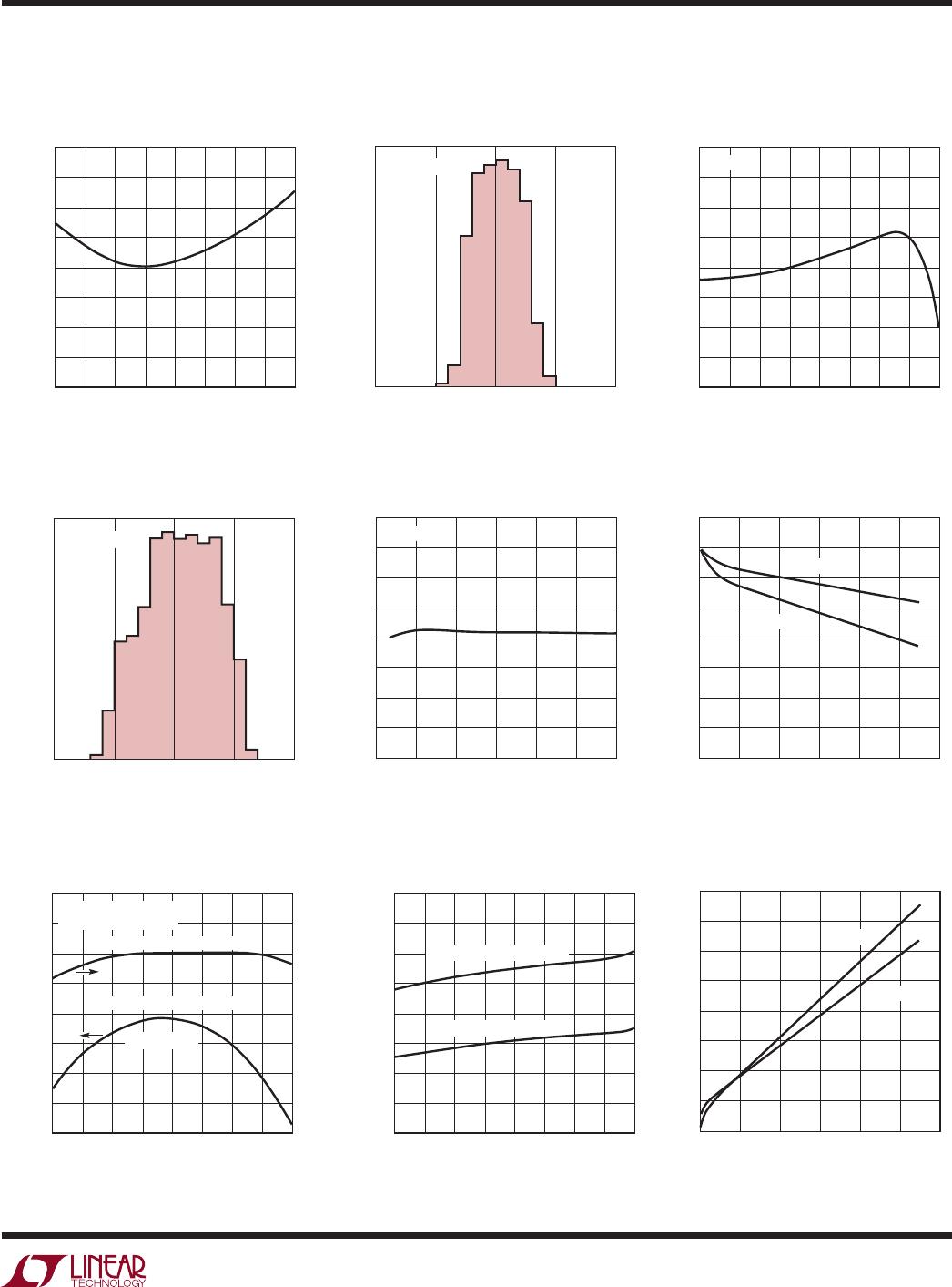
elecTrical characTerisTics
The l denotes the specifications which apply over the full operating
temperature range, otherwise specifications are at T
A
= 25°C. (Note 11)