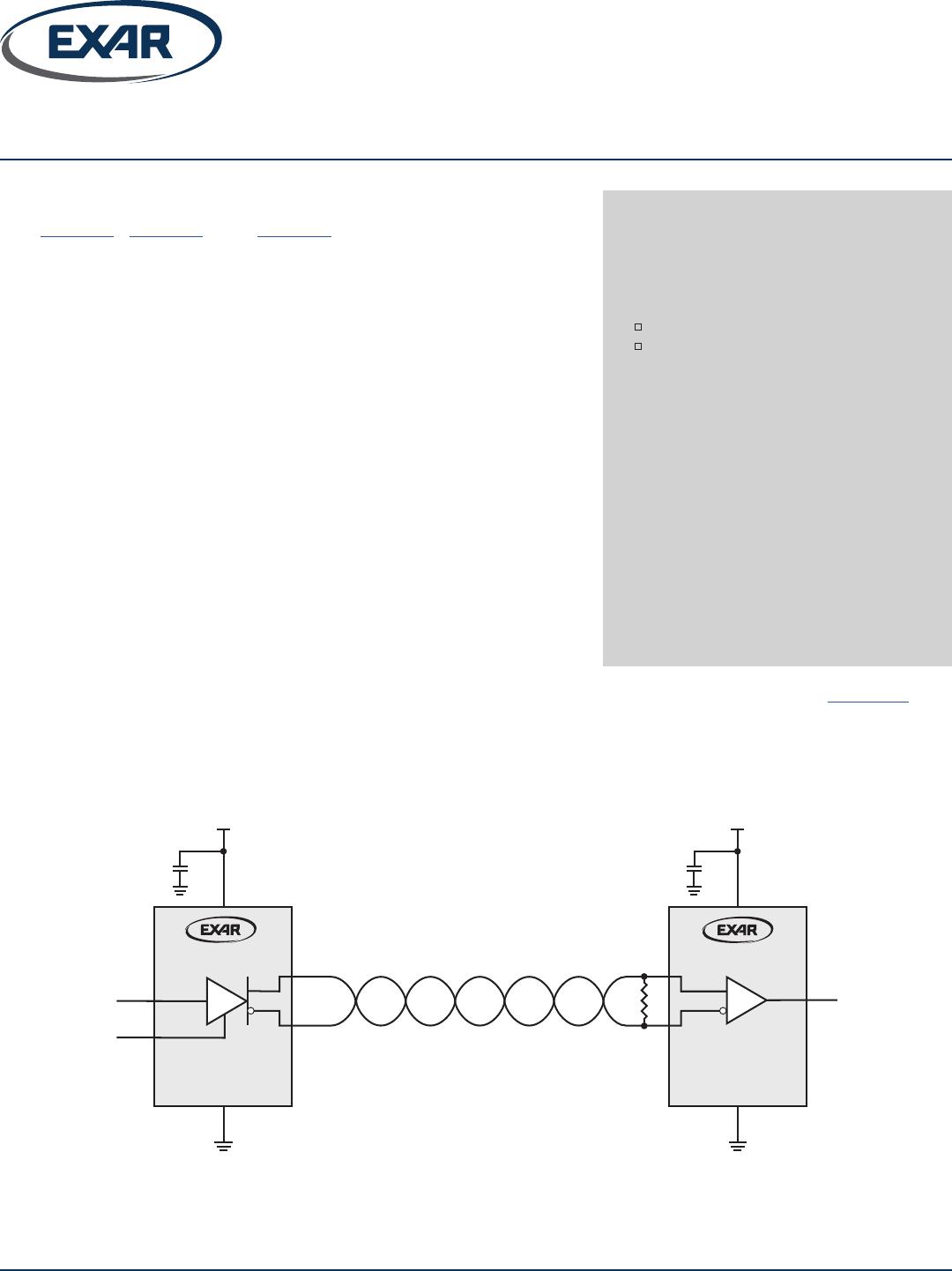
XR33193/94/95
2/12
REV1A
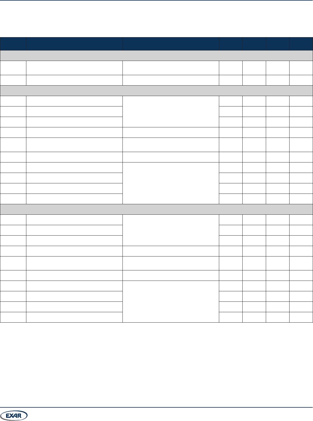
Absolute Maximum Ratings
Stresses beyond the limits listed below may cause
permanent damage to the device. Exposure to any Absolute
Maximum Rating condition for extended periods may affect
device reliability and lifetime.
Supply voltage (V
CC
) ...................................... -0.3V to 7.0V
Maximum junction temperature ................................. 150°C
Input voltages, DI and DE ............................... -0.3V to 7.0V
Bus output voltages Y and Z .......................................±18V
Transient voltage pulse through 100Ω, Figure 7 .......±100V
Operating Conditions
Operating temperature range ...................... -40°C to 125°C
V
CC
supply range .....................................3.135V to 3.465V
Storage temperature range ......................... -65°C to 150°C
Lead temperature (soldering, 10s) ............................ 300°C
Thermal Information
6-pin TSOT23 θ
JA
.............................................. 167.3°C/W
6-pin TSOT23 θ
JC
................................................ 61.6°C/W
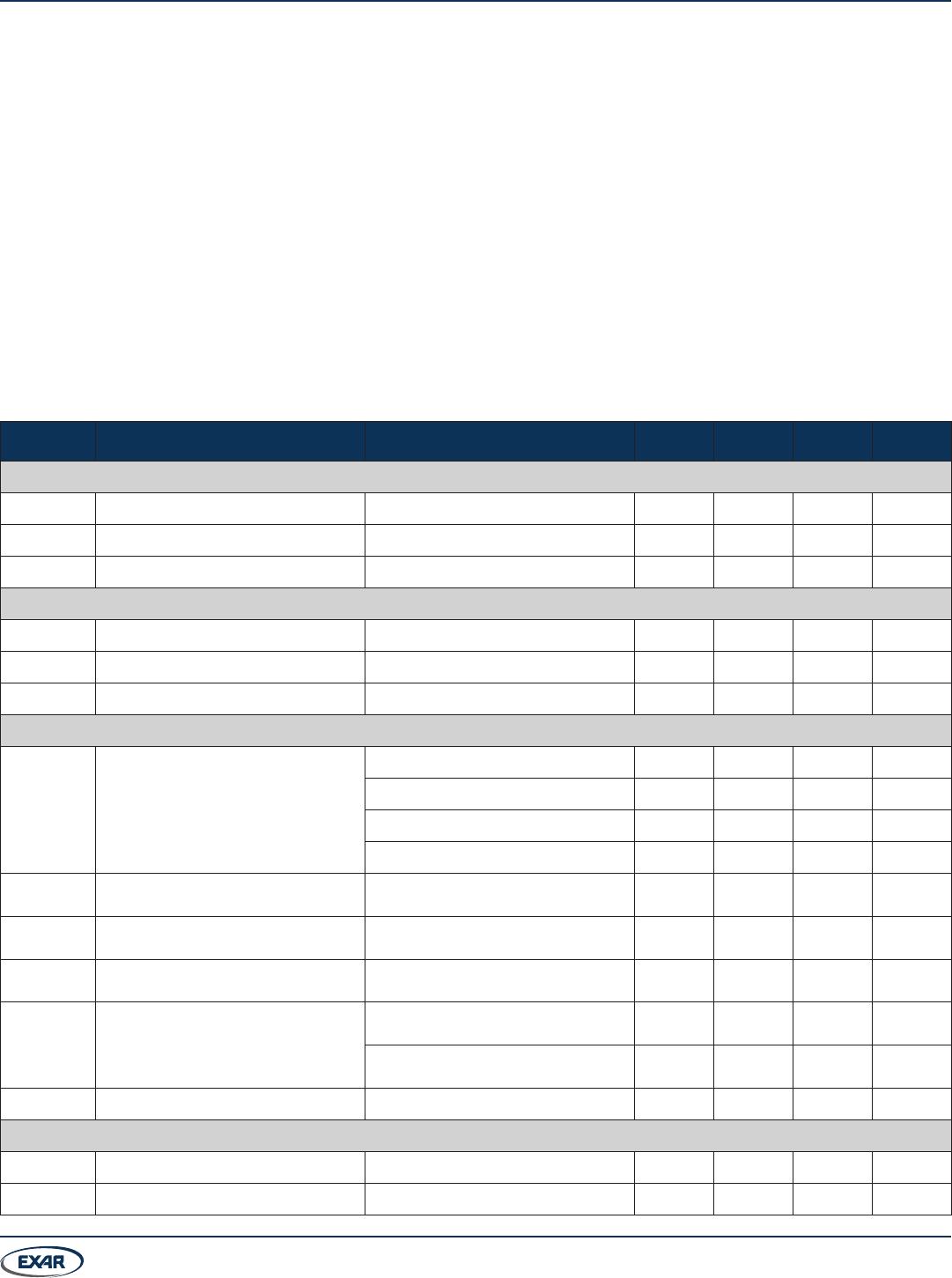
Electrical Characteristics
Specifications are at T
A
= 25°C, V
CC
= 3.3V ± 5% unless otherwise noted. Typical values represent the most likely parametric
norm at T
A
= 25°C, and are provided for reference purposes only.
Symbol Parameter Conditions Min Typ Max Units
Supply
V
CC
Supply voltage range 3.135 3.465 V
I
CC
Supply current No load (DE = V
CC
, DI = 0V) 0.18 0.375 mA
I
SNDN
Supply current in shutdown mode No load (DE = 0V) 0.5 2 µA
Logic Inputs/Outputs
V
IH
Logic high input thresholds DI and DE 2 V
V
IL
Logic high input thresholds DI and DE 0.8 V
I
IN
Input current DI and DE -2 2 µA
Driver DC Characteristics
V
OD
Differential driver voltage
No load 3 V
R
L
= 100Ω (RS-422), Figure 4 2 V
R
L
= 54Ω (RS-485), Figure 4 1.5 V
-7V ≤ V
CM
≤ 12V, Figure 5 1.5 V
∆V
OD
Change in magnitude of differential
driver output voltage
R
L
= 54Ω (RS-485) or 100Ω (RS-422),
DE = V
CC
, Figure 4
±0.2 V
V
CM
Driver common-mode output voltage
(steady state)
R
L
= 54Ω (RS-485) or 100Ω (RS-422),
DE = V
CC
, DI = V
CC
or GND, Figure 4
-1 V
CC
/2 3 V
∆V
CM
Change in magnitude of driver common-
mode output voltage
R
L
= 54Ω (RS-485) or 100Ω (RS-422) 0.2 V
V
OL
Output leakage
Y and Z, V
OUT
= 12V, DE = 0V,
V
CC
= 3.3V or GND
-20 20 µA
Y and Z, V
OUT
= -7V, DE = 0V,
V
CC
= 3.3V or GND
-20 20 µA
I
OSD
Driver short-circuit output current -7V ≤ V
OUT
≤ 12V, Figure 6 ±250 mA
Thermal Characteristics
T
TS
Thermal shutdown temperature 165 °C
T
TSH
Thermal shutdown hysteresis 40 °C