XR33193/94/95
6/12
REV1A
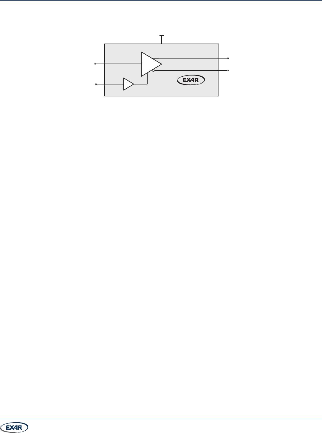
Functional Block Diagram
Figure 2. Functional Block Diagram
Z
V
CC
DI
DE
Y
XR3319x
Applications Information
The XR3319x RS-485/RS-422 devices are part of Exar’s high
performance serial interface product line. These standalone
drivers operate off a single 3.3V supply and meet RS-485 and
RS-422 standards for balanced RS-485 and RS-422 serial
communications networks.
Hot Swap Capability
When V
CC
is first applied the XR3319x family holds the
driver enable inactive for approximately 10μs. During power
ramp-up, other system ICs may drive unpredictable values or
tristated lines may be influenced by stray capacitance. The hot
swap feature prevents the XR3319x family from driving any
output signal until power has stabilized. After the initial 10μs,
the driver enable pin is weakly pulled to the disabled state(low
for DE) until the first transition. After the first transition, the DE
pin operate as high impedance input.
If circuit boards are inserted into an energized backplane
(commonly called “live insertion” or “hot swap”) power
may suddenly be applied to all circuits. Without the hot
swap capability, this situation could improperly enable the
transceiver’s driver, driving invalid data onto shared buses
and possibly causing driver contention or device damage.
Driver Output Protection
Two mechanisms prevent excessive output current and power
dissipation caused by faults or by bus contention. First, a driver
current limit on the output stage provides immediate protection
against short circuits over the whole common-mode voltage
range. Second, a thermal shutdown circuit forces the driver
outputs into a high impedance state if junction temperature
becomes excessive.
Line Length
The RS-485/RS-422 standard covers line lengths up to
4000ft. Maximum achievable line length is a function of
signal attenuation and noise. Termination prevents signal
reflections by eliminating the impedance mismatches on
a transmission line. Line termination is generally used if
rise and fall times are shorter than the round trip signal
propagation time. Higher output drivers may allow longer
cables to be used.
±15kV HBM ESD Protection (Unpowered Part)
ESD protection structures are incorporated on all pins to
protect against electrostatic discharges encountered during
handling and assembly. The driver outputs of the XR3319x
family have extra protection against static electricity.
Exar uses state-of-the-art structures to protect these pins
against ESD damage:
±15kV HBM for bus pins to GND
±4kV HBM for all other pins
ESD Test Conditions
ESD performance depends on a variety of conditions.
Contact Exar for a reliability report that documents test
setup, methodology and results.
Low Power Shutdown Mode
The XR3319x has a low-power shutdown mode that is
initiated by bringing DE low (to disable the XR33193/94/95).
While in shutdown the XR3319x draws less than 2μA of
supply current.