NXP Semiconductors
BGU7045
1 GHz wideband low-noise amplifier with bypass
BGU7045 All information provided in this document is subject to legal disclaimers. © NXP B.V. 2018. All rights reserved.
Product data sheet Rev. 3 — 11 April 2018
3 / 12
4 Marking
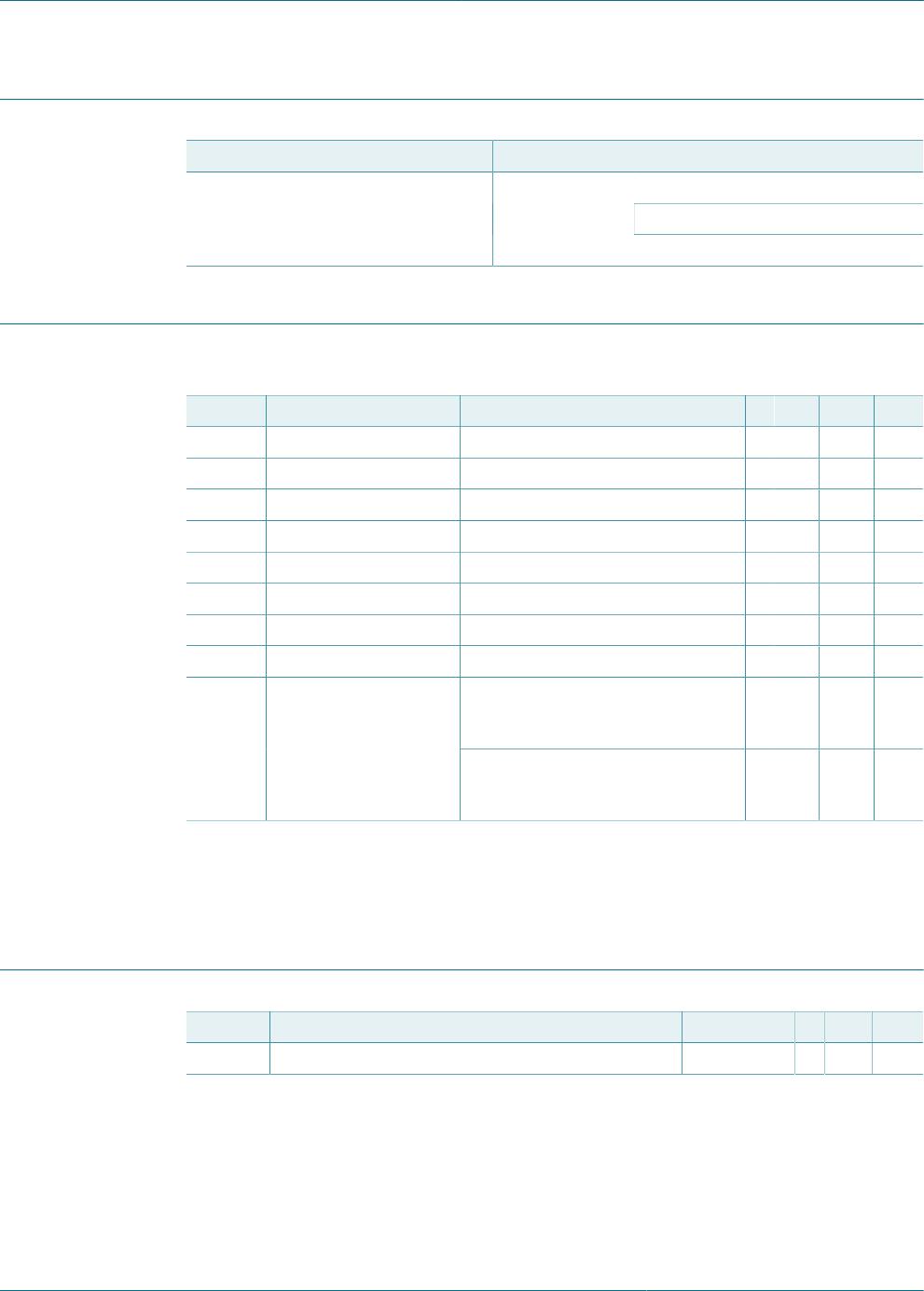
Table 4. Marking code
Type number Marking code Description
* = p: made in Hong Kong
* = W: made in China
BGU7045 LK*
* = t: made in Malaysia
5 Limiting values
Table 5. Limiting values
In accordance with the Absolute Maximum Rating System (IEC 60134).
Symbol Parameter Conditions Min Max Unit
V
CC
supply voltage RF input AC coupled −0.6 3.5 V
V
CTRL
voltage on CTRL pin
[1]
0 V
CC
V
I
CC(tot)
total supply current - 60 mA
P
tot
total power dissipation T
sp
≤ 100 °C
[2]
- 250 mW
P
i
input power single tone - 20 dBm
T
stg
storage temperature −65 +150 °C
T
j
junction temperature - 150 °C
T
amb
ambient temperature −40 +85 °C
Human Body Model (HBM);
according to JEDEC standard 22-
A114E
2 - kVV
ESD
electrostatic discharge
voltage
Charged Device Model (CDM);
according to JEDEC standard 22-
C101B
1.5 - kV
[1] V
CTRL
must not exceed V
CC
; I
CTRL
must be limited to 5 mA (maximum).
[2] T
sp
is the temperature at the solder point of the ground lead.
Remark: V
CTRL
must not exceed V
CC
; I
CTRL
must be limited to a maximum of 5 mA.
6 Thermal characteristics
Table 6. Thermal characteristics
Symbol Parameter Conditions Typ Unit
R
th(j-sp)
thermal resistance from junction to solder point
[1]
130 K/W
[1] Determined by final element method simulation with device mounted on application board and in still air.