NXP Semiconductors
BGU7045
1 GHz wideband low-noise amplifier with bypass
BGU7045 All information provided in this document is subject to legal disclaimers. © NXP B.V. 2018. All rights reserved.
Product data sheet Rev. 3 — 11 April 2018
4 / 12
7 Characteristics
Table 7. Characteristics
T
amb
= 25 °C; typical values at V
CC
= 3.3 V; Z
S
= Z
L
= 75 Ω; R
bias
= 18 Ω; 40 MHz ≤ f
1
≤ 1000 MHz.
Symbol Parameter Conditions Min Typ Max Unit
V
CC
supply voltage RF input AC coupled 3.1 3.3 3.5 V
G
p
= 14 dB mode
[1]
30 34 38 mAI
CC(tot)
total supply current
bypass mode
[1]
- 3 - mA
G
p
= 14 dB mode
[1]
- 14 - dB|s
21
|
2
insertion power gain
bypass mode
[1]
- −2 - dB
SL
sl
slope straight line G
p
= 14 dB mode - −1 - dB
FL flatness of frequency response G
p
= 14 dB mode - 0.2 - dB
G
p
= 14 dB mode
[1]
- 2.8 - dBNF noise figure
bypass mode
[1]
- 2.5 - dB
G
p
= 14 dB mode
[1]
- 20 - dBRL
in
input return loss
bypass mode
[1]
- 9 - dB
G
p
= 14 dB mode
[1]
- 12 - dBRL
out
output return loss
bypass mode
[1]
- 10 - dB
P
L(1dB)
output power at 1 dB gain
compression
G
p
= 14 dB mode; 1
GHz
[1]
- 13 - dBm
G
p
= 14 dB mode
[1][2]
- 29 - dBmIP3
O
output third-order intercept point
bypass mode
[1][2]
- 27 - dBm
[1] Mode depends on setting of V
CTRL
; see Table 8.
[2] The fundamental frequency (f
1
) is 1000 MHz. The intermodulation product (IM3) is 2 × f
2
- f
1
, where f
2
= f
1
± 1 MHz. Input
power P
i
= -10 dBm.
Table 8. Gain selection (pin CTRL)
-10 °C ≤ T
amb
≤ +70 °C; recommended power-up condition: V
CTRL
= logic 0 or < 0.7 V.
V
CTRL
(V) Mode
≤ 0.7 bypass
≥ 1.5 G
p
= 14 dB
Remark: V
CTRL
must not exceed V
CC
; I
CTRL
must be limited to a maximum of 5 mA.
NXP Semiconductors
BGU7045
1 GHz wideband low-noise amplifier with bypass
BGU7045 All information provided in this document is subject to legal disclaimers. © NXP B.V. 2018. All rights reserved.
Product data sheet Rev. 3 — 11 April 2018
5 / 12
8 Application information
Application notes are available on the NXP website.
Section 8.1 describes the application circuit used for characterisation and datasheet.
Section 8.2 describes the recommended application circuit.
8.1 Application circuit
001aam383
C4
C5
R2
3
n.c.
CTRL
2
5
4
16
RF_OUTRF_IN
V
CC
L1
R1 = R
bias
C1X1 C2
C3
X2
Components are listed in Table 9.
Figure 1. BGU7045 application circuit
All control and supply lines must be decoupled properly. The decoupling capacitors must
be placed as close to the device as possible.
8.2 Recommended application circuit
Recommended application circuit to compensate capacitive load influence at RF input.
aaa-029221
C4
C5
R2
3
n.c.
CTRL
2
5
4
16
RF_OUTRF_IN
V
CC
L1
R1 = R
bias
C1
C6
R3
L2
X1 C2
C3
X2
components are listed in Table 10
Figure 2. BGU7045 recommended application circuit.
(Values can be changed depending on the PCB routing) Keep the components (L2, R3,
C6) next to the BGU7045 RF input pin.
NXP Semiconductors
BGU7045
1 GHz wideband low-noise amplifier with bypass
BGU7045 All information provided in this document is subject to legal disclaimers. © NXP B.V. 2018. All rights reserved.
Product data sheet Rev. 3 — 11 April 2018
6 / 12
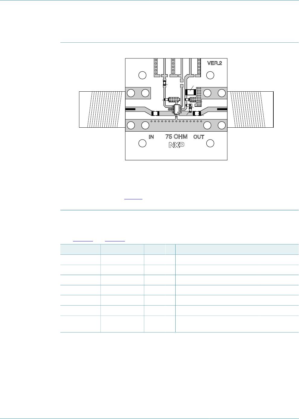
8.3 Application circuit board layout
001aan459
X1 X2
C5
R2
C3
C1
C2
L1
R1
C4
RF_OUTRF_IN
G
N
D
C
T
R
L
BPCTR
L
GAIN CT
R
L
VC
C
G
N
D
V
C
C
G
N
D
PCB material = FR4.
PCB thickness = 1.6 mm.
PCB size = 30 mm x 30 mm.
ε
r
= 4.5; thickness of copper layer = 35 µm.
Components are listed in Table 9.
Figure 3. BGU7045 application circuit board layout.
Table 9. List of components
See Figure 1 and Figure 3 .
Component Description Value Remarks Function
C1, C2 capacitor 10 nF DC blocking
C3, C4 capacitor 10 nF decoupling
C5 capacitor 10 µF decoupling
L1 chip ferrite bead 1.5 kΩ
[1]
Murata BLM18HE152SN1DF RF choke
R1 resistor 18 Ω
[1]
R
bias
bias setting
R2 resistor 1.8 kΩ current limiting
X1, X2 connector 75 Ω F-connector, edge mount PCB
reflow type, Bomar 861V509ER6
input/output
[1] L1 and R1 must have a power rating of 0.1 W or higher.

BGU7045,115

Mfr. #:
Manufacturer:
NXP Semiconductors
Description:
RF Amplifier 1 GHz wideband low noise amp w/ bypass
Lifecycle:
New from this manufacturer.
Delivery:
DHL FedEx Ups TNT EMS
Payment:
T/T Paypal Visa MoneyGram Western Union

Products related to this Datasheet