REV. E
–3–
AD7660
Parameter Conditions Min Typ Max Unit
TEMPERATURE RANGE
Specified Performance T
MIN
to T
MAX
–40 +85 C
NOTES
1
LSB means least significant bit. With the 0 V to 2.5 V input range, one LSB is 38.15 mV.
2
Typical rms noise at worst-case transitions and temperatures.
3
See Definition of Specifications section. These specifications do not include the error contribution from the external reference.
4
All specifications in dB are referred to a full-scale input FS. Tested with an input signal at 0.5 dB below full-scale unless otherwise specified.
5
Tested in Parallel Reading Mode.
6
With all digital inputs forced to DVDD or DGND respectively.
Specifications subject to change without notice.
(–40C to +85C, AVDD = DVDD
= 5 V, OVDD = 2.7 V to 5.25 V, unless otherwise noted.)
TIMING SPECIFICATIONS
Parameter
Symbol Min Typ Max Unit
REFER TO FIGURES 11 AND 12
Convert Pulsewidth t
1
5ns
Time between Conversions t
2
10 ms
CNVST LOW to BUSY HIGH Delay t
3
15 ns
BUSY HIGH All Modes Except in t
4
2 ms
Master Serial Read after Convert Mode
Aperture Delay t
5
2ns
End of Conversion to BUSY LOW Delay t
6
10 ns
Conversion Time t
7
2 ms
Acquisition Time t
8
8 ms
RESET Pulsewidth t
9
10 ns
REFER TO FIGURES 13, 14, AND 15 (Parallel Interface Modes)
CNVST LOW to DATA Valid Delay t
10
2 ms
DATA Valid to BUSY LOW Delay t
11
45 ns
Bus Access Request to DATA Valid t
12
40 ns
Bus Relinquish Time t
13
515ns
REFER TO FIGURE 16 AND 17 (Master Serial Interface Modes)
1
CS LOW to SYNC Valid Delay t
14
10 ns
CS LOW to Internal SCLK Valid Delay t
15
10 ns
CS LOW to SDOUT Delay t
16
10 ns
CNVST LOW to SYNC Delay t
17
500 ns
SYNC Asserted to SCLK First Edge Delay t
18
4ns
Internal SCLK Period t
19
40 75 ns
Internal SCLK HIGH (INVSCLK Low)
2
t
20
30 ns
Internal SCLK LOW (INVSCLK Low)
2
t
21
9.5 ns
SDOUT Valid Setup Time t
22
4.5 ns
SDOUT Valid Hold Time t
23
3ns
SCLK Last Edge to SYNC Delay t
24
3
CS HIGH to SYNC HI-Z t
25
10 ns
CS HIGH to Internal SCLK HI-Z t
26
10 ns
CS HIGH to SDOUT HI-Z t
27
10 ns
BUSY HIGH in Master Serial Read after Convert t
28
3.2 ms
CNVST LOW to SYNC Asserted Delay t
29
1.5 ms
SYNC Deasserted to BUSY LOW Delay t
30
50 ns
REFER TO FIGURES 18 AND 20 (Slave Serial Interface Modes)
1
External SCLK Setup Time t
31
5ns
External SCLK Active Edge to SDOUT Delay t
32
316ns
SDIN Setup Time t
33
5ns
SDIN Hold Time t
34
5ns
External SCLK Period t
35
25 ns
External SCLK HIGH t
36
10 ns
External SCLK LOW t
37
10 ns
NOTES
1
In serial interface modes, the SYNC, SCLK, and SDOUT timings are defined with a maximum load C
L
of 10 pF; otherwise, the load is 60 pF maximum.
2
If the polarity of SCLK is inverted, the timing references of SCLK are also inverted.
Specifications subject to change without notice.
REV. E
AD7660
–4–
ABSOLUTE MAXIMUM RATINGS
1
Analog Inputs
IN
2
, REF, INGND, REFGND . . . . . . . . . . . . . . . . . . . . . .
. . . . . . . . . . . . . . . . . . AVDD + 0.3 V to AGND – 0.3 V
Ground Voltage Differences
AGND, DGND, OGND . . . . . . . . . . . . . . . . . . . . . ± 0.3 V
Supply Voltages
AVDD, DVDD, OVDD . . . . . . . . . . . . . . . . –0.3 V to +7 V
AVDD to DVDD,
AVDD to OVDD . . . . . . . . . . . . . ± 7 V
DVDD to OVDD . . . . . . . . . . . . . . . . . . . . . . . . . . . . ± 7 V
Digital Inputs
Except the Databus D(7:4) . . . –0.3 V to DVDD + 0.3 V
Databus Inputs D(7:4) . . . . . . –0.3 V to OVDD + 0.3 V
Internal Power Dissipation
3
. . . . . . . . . . . . . . . . . . . 700 mW
Internal Power Dissipation
4
. . . . . . . . . . . . . . . . . . . . . 2.5 W
Junction Temperature . . . . . . . . . . . . . . . . . . . . . . . . . 150C
Storage Temperature Range . . . . . . . . . . . . –65C to +150C
Lead Temperature Range
(Soldering 10 sec) . . . . . . . . . . . . . . . . . . . . . . . . . . 300C
NOTES
1
Stresses above those listed under Absolute Maximum Ratings may cause perma-
nent damage to the device. This is a stress rating only; functional operation of the
device at these or any other conditions above those indicated in the operational
section of this specification is not implied. Exposure to absolute maximum rating
conditions for extended periods may affect device reliability.
2
See Analog Input section.
3
Specification is for device in free air: 48-Lead LQFP: q
JA
= 91C/W, q
JC
= 30C/W.
4
Specification is for device in free air: 48-Lead LFCSP: q
JA
= 26C/W.
I
OH
500A
1.6mA I
OL
TO OUTPUT
PIN
1.4V
C
L
60pF
*
*IN SERIAL INTERFACE MODES, THE SYNC, SCLK, AND
SDOUT TIMINGS ARE DEFINED WITH A MAXIMUM LOAD
C
L
OF 10pF; OTHERWISE, THE LOAD IS 60pF MAXIMUM.
Figure 1. Load Circuit for Digital Interface Timing
PIN CONFIGURATION
t
DELAY
t
DELAY
0.8V
0.8V 0.8V
2V2V
2V
Figure 2. Voltage Reference Levels for Timings
CAUTION
ESD (electrostatic discharge) sensitive device. Electrostatic charges as high as 4000 V readily
accumulate on the human body and test equipment and can discharge without detection. Although
the AD7660 features proprietary ESD protection circuitry, permanent damage may occur on
devices subjected to high energy electrostatic discharges. Therefore, proper ESD precautions are
recommended to avoid performance degradation or loss of functionality.
WARNING!
ESD SENSITIVE DEVICE
ORDERING GUIDE
Model
1
Temperature Range Package Description Package Option
–40C to +85C ST-48
–40C to +85C ST-48
–40C to +85C
AD7660ASTZ
AD7660ASTZRL
AD7660ACPZRL
NOTES
1
Z = RoHS Compliant Part.
CP-48-4
48-Lead LQFP
48-Lead LQFP
48-Lead LFCSP
AGND
AVDD
NC
DGND
OB/2C
NC
NC
SER/PAR
D0
D1
D2
D3
AGND
CNVST
PD
RESET
CS
RD
DGND
BUSY
D15
D14
D13
D12
D4/EXT/INT
D5/INVSYNC
D6/INVSCLK
D7/RDC/SDIN
OGND
OVDD
DVDD
DGND
D8/SDOUT
D9/SCLK
D10/SYNC
D11/RDERROR
NC
NC
NC
NC
NC
IN
NC
NC
NC
INGND
REFGND
REF
24
23
22
21
20
19
18
17
1
6
15
14
13
44
45
46
47
48
43
42
41
40
39
38
37
AD7660
TOP VIEW
(Not to Scale)
25
26
27
28
29
30
31
32
33
34
35
36
1
2
3
4
5
6
7
8
9
10
11
12
NOTES
1. NC = NO CONNECT. DO NOT CONNECT TO THIS PIN.
2. THE EPAD IS CONNECTED TO GROUND; HOWEVER,
THIS CONNECTION IS NOT REQUIRED TO MEET
SPECIFIED PERFORMANCE.
REV. E
AD7660
–5–
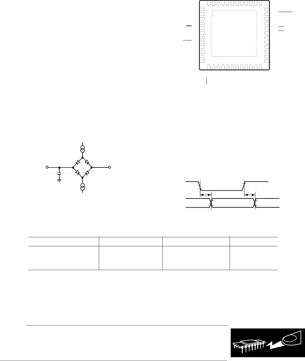
PIN FUNCTION DESCRIPTIONS
Pin
No. Mnemonic Type Description
1 AGND P Analog Power Ground Pin
2 AVDD P Input Analog Power Pins. Nominally 5 V.
3, 6, 7, NC No Connect
40–42,
44–48
4 DGND DI Must Be Tied to Digital Ground
5OB/2C DI Straight Binary/Binary Twos Complement. When OB/2C is HIGH, the digital output is
straight binary; when LOW, the MSB is inverted resulting in a twos complement output from
its internal shift register.
8 SER/PAR DI Serial/Parallel Selection Input. When LOW, the Parallel Port is selected; when HIGH, the
Serial Interface Mode is selected and some bits of the DATA bus are used as a Serial Port.
9–12 D[0:3] DO Bit 0 to Bit 3 of the Parallel Port Data Output Bus. These pins are always outputs regardless
of the state of SER/PAR.
13 D4 DI/O When SER/PAR is LOW, this output is used as the Bit 4 of the Parallel Port Data Output Bus.
or EXT/INT When SER/PAR is HIGH, this input, part of the Serial Port, is used as a digital select input
for choosing the internal or an external data clock. With EXT/INT tied LOW, the internal
clock is selected on the SCLK output. With EXT/INT set to a logic HIGH, output data is
synchronized to an external clock signal connected to the SCLK input.
14 D5 DI/O When SER/PAR is LOW, this output is used as the Bit 5 of the Parallel Port Data Output Bus.
or INVSYNC When SER/PAR is HIGH, this input, part of the Serial Port, is used to select the active state
of the SYNC signal. When LOW, SYNC is active HIGH. When HIGH, SYNC is active LOW.
15 D6 DI/O When SER/PAR is LOW, this output is used as the Bit 6 of the Parallel Port Data Output Bus.
or INVSCLK When SER/PAR is HIGH, this input, part of the Serial Port, is used to invert the SCLK
signal. It is active in both Master and Slave Modes.
16 D7 DI/O When SER/PAR is LOW, this output is used as the Bit 7 of the Parallel Port Data Output Bus.
or RDC/SDIN When SER/PAR is HIGH, this input, part of the Serial Port, is used as either an external data
input or a Read Mode selection input depending on the state of EXT/INT.
When EXT/INT is HIGH, RDC/SDIN could be used as a data input to daisy-chain the
conversion results from two or more ADCs onto a single SDOUT line. The digital data level
on SDIN is output on DATA with a delay of 16 SCLK periods after the initiation of the read
sequence.
When EXT/INT is LOW, RDC/SDIN is used to select the Read Mode. When RDC/SDIN is
HIGH, the data is output on SDOUT during conversion. When RDC/SDIN is LOW, the
data is output on SDOUT only when the conversion is complete.
17 OGND P Input/Output Interface Digital Power Ground
18 OVDD P Input/Output Interface Digital Power. Nominally at the same supply as the supply of the host
interface (5 V or 3 V).
19 DVDD P Digital Power. Nominally at 5 V.
20 DGND P Digital Power Ground
21 D8 DO When SER/PAR is LOW, this output is used as Bit 8 of the Parallel Port Data Output Bus.
or SDOUT When SER/PAR is HIGH, this output, part of the Serial Port, is used as a serial data output
synchronized to SCLK. Conversion results are stored in an on-chip register. The AD7660
provides the conversion result, MSB first, from its internal shift register. The DATA format
is determined by the logic level of OB/2C. In Serial Mode, when EXT/INT is LOW, SDOUT
is valid on both edges of SCLK.
In Serial Mode, when EXT/INT is HIGH:
If INVSCLK is LOW, SDOUT is updated on the SCLK rising edge and valid on the next
falling edge.
If INVSCLK is HIGH, SDOUT is updated on the SCLK falling edge and valid on the next
rising edge.

AD7660ASTZ

Mfr. #:
Manufacturer:
Analog Devices Inc.
Description:
Analog to Digital Converters - ADC 16B 100kSPS CMOS Successive Approx
Lifecycle:
New from this manufacturer.
Delivery:
DHL FedEx Ups TNT EMS
Payment:
T/T Paypal Visa MoneyGram Western Union

Products related to this Datasheet